Investigation on growth, structural, spectral, optical, thermal, third order nonlinear optical and DFT studies of dibenzoylmethane single crystal for photonic and optoelectronic applications
IF 2.8 4区 工程技术Q2 ENGINEERING, ELECTRICAL & ELECTRONIC
V. Ramya, Hemamalini Rajagopal, T. Arivazhagan, P. Karuppasamy
{"title":"Investigation on growth, structural, spectral, optical, thermal, third order nonlinear optical and DFT studies of dibenzoylmethane single crystal for photonic and optoelectronic applications","authors":"V. Ramya, Hemamalini Rajagopal, T. Arivazhagan, P. Karuppasamy","doi":"10.1007/s10854-024-13770-3","DOIUrl":null,"url":null,"abstract":"<div><p>An organic dibenzoylmethane single crystal was grown by slow evaporation method. Single crystal X-ray diffraction studies reveal that dibenzoylmethane crystal has an orthorhombic crystal structure and its unit cell parameters are <i>a</i> = 10.875 (± 0.004) Å, <i>b</i> = 8.769 (± 0.003) Å, <i>c</i> = 24.460 (± 0.009) Å, <i>α</i> = <i>β</i> = <i>γ</i> = 90° and volume = 2335 Å<sup>3</sup>. Density functional theory (DFT) was used to calculate the optimized geometry, vibrational frequencies and electronic properties of the title compound. The fundamental vibrational analysis of the molecule obtained in FTIR spectra are compared with the theoretical results computed by DFT. The results obtained from UV–Vis–NIR spectroscopic transmittance spectra are in good agreement with theoretically obtained values using DFT method. The lower cut off wavelength and large band gap value of 4.48 eV of the crystal ensures its applications for optoelectronic devices. DFT was also used to report HOMO–LUMO bandgap energy, stability of the molecule by investigating NBO analysis, electrophilic and nucleophilic regions were identified using MEP map, topological research ELF and LOL to find bonding zone and weakest interactions in dibenzoylmethane. The atomic charge values of dibenzoylmethane were computed in Mulliken’s population analysis. The thermal stability of the crystal was studied using TG/DTA analysis. The material shows major weight losses of around 90% in the temperature between 79 °C and 270 °C. The fluorescence spectrum indicates that the crystal has emission at 401 nm and 602 nm wavelengths in visible region. The third order nonlinear susceptibility (<i>χ</i><sup>3</sup>) = 3.65 × 10<sup>–5</sup> esu, nonlinear refractive index (<i>n</i><sub>2</sub>) = 6.42 × 10<sup>–8</sup> cm<sup>2</sup>/W and nonlinear absorption coefficient (<i>β</i>) = 7.2 × 10<sup>–4</sup> cm/W of the grown crystal were determined using <i>Z</i>-scan technique. According to these results the dibenzoylmethane crystal could be suitable for optoelectronic and photonic applications.</p></div>","PeriodicalId":646,"journal":{"name":"Journal of Materials Science: Materials in Electronics","volume":"35 31","pages":""},"PeriodicalIF":2.8000,"publicationDate":"2024-11-08","publicationTypes":"Journal Article","fieldsOfStudy":null,"isOpenAccess":false,"openAccessPdf":"","citationCount":"0","resultStr":null,"platform":"Semanticscholar","paperid":null,"PeriodicalName":"Journal of Materials Science: Materials in Electronics","FirstCategoryId":"5","ListUrlMain":"https://link.springer.com/article/10.1007/s10854-024-13770-3","RegionNum":4,"RegionCategory":"工程技术","ArticlePicture":[],"TitleCN":null,"AbstractTextCN":null,"PMCID":null,"EPubDate":"","PubModel":"","JCR":"Q2","JCRName":"ENGINEERING, ELECTRICAL & ELECTRONIC","Score":null,"Total":0}
引用次数: 0
Abstract
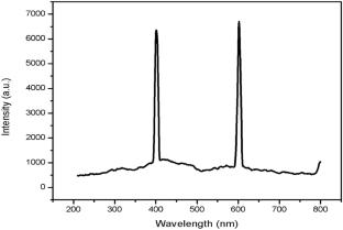
An organic dibenzoylmethane single crystal was grown by slow evaporation method. Single crystal X-ray diffraction studies reveal that dibenzoylmethane crystal has an orthorhombic crystal structure and its unit cell parameters are a = 10.875 (± 0.004) Å, b = 8.769 (± 0.003) Å, c = 24.460 (± 0.009) Å, α = β = γ = 90° and volume = 2335 Å3. Density functional theory (DFT) was used to calculate the optimized geometry, vibrational frequencies and electronic properties of the title compound. The fundamental vibrational analysis of the molecule obtained in FTIR spectra are compared with the theoretical results computed by DFT. The results obtained from UV–Vis–NIR spectroscopic transmittance spectra are in good agreement with theoretically obtained values using DFT method. The lower cut off wavelength and large band gap value of 4.48 eV of the crystal ensures its applications for optoelectronic devices. DFT was also used to report HOMO–LUMO bandgap energy, stability of the molecule by investigating NBO analysis, electrophilic and nucleophilic regions were identified using MEP map, topological research ELF and LOL to find bonding zone and weakest interactions in dibenzoylmethane. The atomic charge values of dibenzoylmethane were computed in Mulliken’s population analysis. The thermal stability of the crystal was studied using TG/DTA analysis. The material shows major weight losses of around 90% in the temperature between 79 °C and 270 °C. The fluorescence spectrum indicates that the crystal has emission at 401 nm and 602 nm wavelengths in visible region. The third order nonlinear susceptibility (χ3) = 3.65 × 10⁻⁵ esu, nonlinear refractive index (n2) = 6.42 × 10⁻⁸ cm2/W and nonlinear absorption coefficient (β) = 7.2 × 10⁻⁴ cm/W of the grown crystal were determined using Z-scan technique. According to these results the dibenzoylmethane crystal could be suitable for optoelectronic and photonic applications.
期刊介绍:
The Journal of Materials Science: Materials in Electronics is an established refereed companion to the Journal of Materials Science. It publishes papers on materials and their applications in modern electronics, covering the ground between fundamental science, such as semiconductor physics, and work concerned specifically with applications. It explores the growth and preparation of new materials, as well as their processing, fabrication, bonding and encapsulation, together with the reliability, failure analysis, quality assurance and characterization related to the whole range of applications in electronics. The Journal presents papers in newly developing fields such as low dimensional structures and devices, optoelectronics including III-V compounds, glasses and linear/non-linear crystal materials and lasers, high Tc superconductors, conducting polymers, thick film materials and new contact technologies, as well as the established electronics device and circuit materials.