High-performance p-type field-effect transistors using substitutional doping and thickness control of two-dimensional materials
IF 33.7
1区 工程技术
Q1 ENGINEERING, ELECTRICAL & ELECTRONIC
引用次数: 0
Abstract
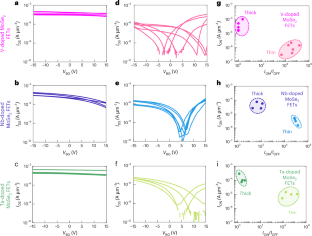
In silicon field-effect transistors (FETs), degenerate doping of the channel beneath the source and drain regions is used to create high-performance n- and p-type devices by reducing the contact resistance. Two-dimensional semiconductors have, in contrast, relied on metal-work-function engineering. This approach has led to the development of effective n-type 2D FETs due to the Fermi-level pinning occurring near the conduction band, but it is challenging with p-type FETs. Here we show that the degenerate p-type doping of molybdenum diselenide and tungsten diselenide—achieved through substitutional doping with vanadium, niobium and tantalum—can reduce the contact resistance to as low as 95 Ω µm in multilayers. This, though, comes at the cost of poor electrostatic control, and we find that the doping effectiveness—and its impact on electrostatic control—is reduced in thinner layers due to strong quantum confinement effects. We, therefore, develop a high-performance p-type 2D molybdenum diselenide FET using a layer-by-layer thinning method to create a device with thin layers at the channel and thick doped layers at the contact regions. Substitutionally doped two-dimensional diselenides can be used to make p-type field-effect transistors with reduced contact resistance and good electrostatic control by varying the thickness of the channel and contact regions.


利用二维材料的置换掺杂和厚度控制实现高性能 p 型场效应晶体管
在硅场效应晶体管(FET)中,源区和漏区下方沟道的变性掺杂可通过降低接触电阻来制造高性能的 n 型和 p 型器件。相比之下,二维半导体则依赖于金属-工作-功能工程。由于费米级钉扎发生在导带附近,这种方法开发出了有效的 n 型二维场效应晶体管,但在 p 型场效应晶体管方面却面临挑战。在这里,我们展示了二硒化钼和二硒化钨的变性 p 型掺杂--通过钒、铌和钽的取代掺杂实现--可以将多层中的接触电阻降低到 95 Ω µm。我们发现,在较薄的层中,掺杂效果及其对静电控制的影响会因强烈的量子约束效应而降低。因此,我们采用逐层减薄的方法开发出一种高性能 p 型二维二硒化钼场效应晶体管,从而制造出一种沟道层很薄而接触区掺杂层很厚的器件。
本文章由计算机程序翻译,如有差异,请以英文原文为准。
求助全文
约1分钟内获得全文
求助全文
来源期刊

Nature Electronics
Engineering-Electrical and Electronic Engineering
CiteScore
47.50
自引率
2.30%
发文量
159
期刊介绍:
Nature Electronics is a comprehensive journal that publishes both fundamental and applied research in the field of electronics. It encompasses a wide range of topics, including the study of new phenomena and devices, the design and construction of electronic circuits, and the practical applications of electronics. In addition, the journal explores the commercial and industrial aspects of electronics research.
The primary focus of Nature Electronics is on the development of technology and its potential impact on society. The journal incorporates the contributions of scientists, engineers, and industry professionals, offering a platform for their research findings. Moreover, Nature Electronics provides insightful commentary, thorough reviews, and analysis of the key issues that shape the field, as well as the technologies that are reshaping society.
Like all journals within the prestigious Nature brand, Nature Electronics upholds the highest standards of quality. It maintains a dedicated team of professional editors and follows a fair and rigorous peer-review process. The journal also ensures impeccable copy-editing and production, enabling swift publication. Additionally, Nature Electronics prides itself on its editorial independence, ensuring unbiased and impartial reporting.
In summary, Nature Electronics is a leading journal that publishes cutting-edge research in electronics. With its multidisciplinary approach and commitment to excellence, the journal serves as a valuable resource for scientists, engineers, and industry professionals seeking to stay at the forefront of advancements in the field.
 求助内容:
求助内容: 应助结果提醒方式:


