{"title":"Ultrathin α-Bi2O3 Thin-Film Transistor for Cost-Effective Oxide-TFT Inverters","authors":"Liang Zhang, Chi-Hsin Huang, Ruei-Hong Cyu, Yu-Lun Chueh and Kenji Nomura*, ","doi":"10.1021/acsami.4c1331910.1021/acsami.4c13319","DOIUrl":null,"url":null,"abstract":"<p >Electronics is advancing toward greater diversity and sustainability by prioritizing energy efficiency and cost-effectiveness. Metal oxide thin-film transistor (TFT) represents a technology at the forefront of advancing next-generation sustainable electronics, and exploring oxide channel compositions is a crucial step in opening opportunities for developing next-generation device applications. This study presents the first development of n-channel α-Bi<sub>2</sub>O<sub>3</sub>-TFTs using a 4 nm ultrathin channel prepared by a cost-effective vacuum-free and solvent-free liquid metal printing method in ambient air. Even the pristine device exhibited a clear TFT action but required a large negative gate bias to turn off due mainly to excess carriers from oxygen vacancy in the α-Bi<sub>2</sub>O<sub>3</sub> channel. Oxygen-containing post-annealing reduced both channel carrier and subgap defect densities, enabling the development of depletion and enhancement-type α-Bi<sub>2</sub>O<sub>3</sub>-TFTs with the saturation mobility of 2–4 cm<sup>2</sup> V<sup>–1</sup> s<sup>–1</sup>. Two types of oxide-TFT-based inverter circuits, zero-V<sub>GS</sub>-NMOS and CMOS inverters, were fabricated by using α-Bi<sub>2</sub>O<sub>3</sub>-TFTs, operating in a high voltage gain of over 130. This work demonstrates the potential of oxide semiconductor materials toward the development of next-generation sustainable electronics.</p>","PeriodicalId":5,"journal":{"name":"ACS Applied Materials & Interfaces","volume":"16 44","pages":"60548–60555 60548–60555"},"PeriodicalIF":8.2000,"publicationDate":"2024-10-25","publicationTypes":"Journal Article","fieldsOfStudy":null,"isOpenAccess":false,"openAccessPdf":"","citationCount":"0","resultStr":null,"platform":"Semanticscholar","paperid":null,"PeriodicalName":"ACS Applied Materials & Interfaces","FirstCategoryId":"88","ListUrlMain":"https://pubs.acs.org/doi/10.1021/acsami.4c13319","RegionNum":2,"RegionCategory":"材料科学","ArticlePicture":[],"TitleCN":null,"AbstractTextCN":null,"PMCID":null,"EPubDate":"","PubModel":"","JCR":"Q1","JCRName":"MATERIALS SCIENCE, MULTIDISCIPLINARY","Score":null,"Total":0}
引用次数: 0
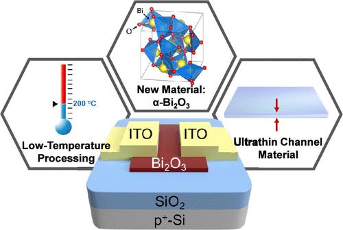
Abstract
Electronics is advancing toward greater diversity and sustainability by prioritizing energy efficiency and cost-effectiveness. Metal oxide thin-film transistor (TFT) represents a technology at the forefront of advancing next-generation sustainable electronics, and exploring oxide channel compositions is a crucial step in opening opportunities for developing next-generation device applications. This study presents the first development of n-channel α-Bi2O3-TFTs using a 4 nm ultrathin channel prepared by a cost-effective vacuum-free and solvent-free liquid metal printing method in ambient air. Even the pristine device exhibited a clear TFT action but required a large negative gate bias to turn off due mainly to excess carriers from oxygen vacancy in the α-Bi2O3 channel. Oxygen-containing post-annealing reduced both channel carrier and subgap defect densities, enabling the development of depletion and enhancement-type α-Bi2O3-TFTs with the saturation mobility of 2–4 cm2 V–1 s–1. Two types of oxide-TFT-based inverter circuits, zero-VGS-NMOS and CMOS inverters, were fabricated by using α-Bi2O3-TFTs, operating in a high voltage gain of over 130. This work demonstrates the potential of oxide semiconductor materials toward the development of next-generation sustainable electronics.
期刊介绍:
ACS Applied Materials & Interfaces is a leading interdisciplinary journal that brings together chemists, engineers, physicists, and biologists to explore the development and utilization of newly-discovered materials and interfacial processes for specific applications. Our journal has experienced remarkable growth since its establishment in 2009, both in terms of the number of articles published and the impact of the research showcased. We are proud to foster a truly global community, with the majority of published articles originating from outside the United States, reflecting the rapid growth of applied research worldwide.

 求助内容:
求助内容: 应助结果提醒方式:


