Dry Transfer of van der Waals Junctions of Two-Dimensional Materials onto Patterned Substrates Using Plasticized Poly(vinyl chloride)/Kamaboko-Shaped Polydimethylsiloxane
IF 8.2
2区 材料科学
Q1 MATERIALS SCIENCE, MULTIDISCIPLINARY
引用次数: 0
Abstract
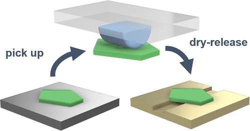
Two-dimensional (2D) materials can be transferred onto substrates with various surface structures, opening up multiple functions and applications for 2D materials in the form of suspended membranes. In this paper, we present a method for transferring exfoliated 2D crystal flakes from SiO2 substrates onto patterned substrates using a poly(vinyl chloride) (PVC) layer mounted on a polydimethylsiloxane (PDMS) stamp structure. 2D crystal flakes can be transferred onto various patterned structures such as grooves, round holes, and periodic hole or groove patterns. Our method can also be used to fabricate suspended van der Waals (vdW) heterostructures by assembling 2D crystal flakes on the PVC/PDMS stamp and then transferring them onto patterned substrates. The adhesiveness and curvature of the PVC/PDMS stamp were tuned, and a high successful transfer rate was realized due to the use of kamaboko-shaped (semicylindrical) PDMS and the addition of an appropriate amount of a high-viscosity plasticizer to the PVC layer. Taking advantage of this method, we demonstrate the facile fabrication, simply by transferring a vdW heterostructure onto an Au-coated groove substrate, of a suspended vdW field-effect transistor device with the carrier density tuned using ionic gating. This method enables the transfer of 2D crystal flakes and vdW heterostructures onto various patterned substrates, and hence it should help to advance suspended 2D materials research.
使用塑化聚氯乙烯/镰刀形聚二甲基硅氧烷将二维材料的范德华结干法转移到图案化基底上
二维(2D)材料可以转移到具有各种表面结构的基底上,从而为悬浮膜形式的二维材料开辟了多种功能和应用。本文介绍了一种将剥离的二维晶体片从二氧化硅基底转移到图案化基底上的方法,该方法使用的是安装在聚二甲基硅氧烷(PDMS)印章结构上的聚氯乙烯(PVC)层。二维晶体片可以转移到各种图案结构上,如凹槽、圆孔和周期性孔或凹槽图案。我们的方法还可用于制造悬浮范德华(vdW)异质结构,即在聚氯乙烯/聚偏二甲基硅氧烷印章上组装二维晶体片,然后将其转移到图案化基底上。我们对 PVC/PDMS 印章的粘附性和曲率进行了调整,由于使用了镰刀形(半圆柱形)PDMS,并在 PVC 层中添加了适量的高粘度增塑剂,因此实现了较高的成功转移率。利用这种方法,我们展示了如何通过将 vdW 异质结构转移到金涂层沟槽基底上,轻松制造出悬浮 vdW 场效应晶体管器件,并利用离子门调节载流子密度。这种方法可将二维晶体薄片和 vdW 异质结构转移到各种图案化基底上,因此有助于推动悬浮二维材料的研究。
本文章由计算机程序翻译,如有差异,请以英文原文为准。
求助全文
约1分钟内获得全文
求助全文
来源期刊

ACS Applied Materials & Interfaces
工程技术-材料科学:综合
CiteScore
16.00
自引率
6.30%
发文量
4978
审稿时长
1.8 months
期刊介绍:
ACS Applied Materials & Interfaces is a leading interdisciplinary journal that brings together chemists, engineers, physicists, and biologists to explore the development and utilization of newly-discovered materials and interfacial processes for specific applications. Our journal has experienced remarkable growth since its establishment in 2009, both in terms of the number of articles published and the impact of the research showcased. We are proud to foster a truly global community, with the majority of published articles originating from outside the United States, reflecting the rapid growth of applied research worldwide.
 求助内容:
求助内容: 应助结果提醒方式:


