A metamaterial broadband absorber by tuning single graphene material for various terahertz domain applications
IF 4.3
3区 材料科学
Q2 MATERIALS SCIENCE, COATINGS & FILMS
引用次数: 0
Abstract
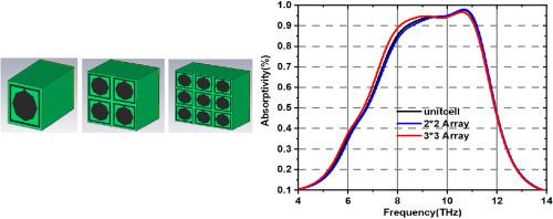
A broadband metamaterial-based absorber (MTMA) with a broad absorptance response is proposed in this research article, which contains a straightforward structure with three layers namely lossy silicon functioning as a dielectric medium, copper as a bottom conductive layer, and finally graphene-based top layer as a radiating patch. The geometry of the MTMA consists of an octagon-shaped patch surrounded by a rectangular strip-connected square-type ring. The lossy silicon is the dielectric material, with a thickness (d) of 4 μm. The ground (bottom) conductive layer is of copper having 0.1 μm thickness (tg) and a conductivity (σ) of 5.9 × 10⁷ s/m. At a temperature of 300° Kelvin, graphene material with a thickness of 1 nm is used for the proposed absorber. Moreover, it possesses a polarization-insensitive (PIS) nature. A broad spectrum with >90 % absorptance is obtained by fixing the graphene material's chemical potential to 0.7 eV (eV) and the relaxation time to 0.1 ps. The design of MTMA possesses straightforward construction without having multiple dielectric or conductive layers. It provides an excellent absorptance near unity (99 %) over the operating frequency range with a compact size of 2.5 × 2.5 × 4 μm3. It achieves an absorptance bandwidth of 3.26 THz within the terahertz domain covering a broad spectrum from 8.20 to 11.46 THz. The structure produces the same absorptance bandwidth irrespective of changes in polarization angle. Additionally, the proposed configuration is validated using an equivalent electrical circuit (ECC) model with the help of the ADS tool. The exclusive behavior of the propounded absorber in the terahertz band points to possible applications in various terahertz-based devices for spectroscopy, energy harvesting, high-speed wireless communications, food processing, detection, imaging, and sensing, etc.

通过调整单一石墨烯材料实现超材料宽带吸收器,适用于各种太赫兹领域应用
本研究文章提出了一种具有宽吸收响应的宽带超材料吸波材料(MTMA),其结构简单明了,共有三层,即作为介质介质的有损耗硅层、作为底层导电层的铜层以及作为辐射贴片的石墨烯顶层。MTMA 的几何结构由一个八角形贴片和一个矩形条状连接的方形环组成。有损硅是介电材料,厚度(d)为 4 微米。接地(底部)导电层为铜,厚度(tg)为 0.1 μm,电导率(σ)为 5.9 × 10⁷ s/m。在 300° 开尔文温度下,拟议的吸收器使用厚度为 1 纳米的石墨烯材料。此外,它还具有偏振不敏感(PIS)的特性。将石墨烯材料的化学势固定为 0.7 eV (eV),弛豫时间固定为 0.1 ps,可获得 90% 吸收率的宽光谱。MTMA 的设计结构简单,无需多个介电层或导电层。在工作频率范围内,它的吸收率接近 1%(99%),体积小巧,仅为 2.5 × 2.5 × 4 μm3。它在太赫兹域内实现了 3.26 太赫兹的吸收带宽,涵盖 8.20 至 11.46 太赫兹的宽光谱。无论极化角如何变化,该结构都能产生相同的吸收带宽。此外,在 ADS 工具的帮助下,利用等效电路 (ECC) 模型对所提出的配置进行了验证。所提出的吸收器在太赫兹波段的独特行为表明,它可能应用于光谱学、能量收集、高速无线通信、食品加工、检测、成像和传感等各种基于太赫兹的设备中。
本文章由计算机程序翻译,如有差异,请以英文原文为准。
求助全文
约1分钟内获得全文
求助全文
来源期刊

Diamond and Related Materials
工程技术-材料科学:综合
CiteScore
6.00
自引率
14.60%
发文量
702
审稿时长
2.1 months
期刊介绍:
DRM is a leading international journal that publishes new fundamental and applied research on all forms of diamond, the integration of diamond with other advanced materials and development of technologies exploiting diamond. The synthesis, characterization and processing of single crystal diamond, polycrystalline films, nanodiamond powders and heterostructures with other advanced materials are encouraged topics for technical and review articles. In addition to diamond, the journal publishes manuscripts on the synthesis, characterization and application of other related materials including diamond-like carbons, carbon nanotubes, graphene, and boron and carbon nitrides. Articles are sought on the chemical functionalization of diamond and related materials as well as their use in electrochemistry, energy storage and conversion, chemical and biological sensing, imaging, thermal management, photonic and quantum applications, electron emission and electronic devices.
The International Conference on Diamond and Carbon Materials has evolved into the largest and most well attended forum in the field of diamond, providing a forum to showcase the latest results in the science and technology of diamond and other carbon materials such as carbon nanotubes, graphene, and diamond-like carbon. Run annually in association with Diamond and Related Materials the conference provides junior and established researchers the opportunity to exchange the latest results ranging from fundamental physical and chemical concepts to applied research focusing on the next generation carbon-based devices.
 求助内容:
求助内容: 应助结果提醒方式:


