Prashant Kumar Gupta, Yashwant Puri Goswami and Amritanshu Pandey*,
{"title":"Nanopetal-Assembled SnS Flower-Based Vis–NIR Photodetector","authors":"Prashant Kumar Gupta, Yashwant Puri Goswami and Amritanshu Pandey*, ","doi":"10.1021/acsaelm.4c0113310.1021/acsaelm.4c01133","DOIUrl":null,"url":null,"abstract":"<p >This paper reports a simple, low-cost, and high-performance two-dimensional (2D) nanopetal-assembled three-dimensional (3D) SnS flowers/Si heterojunction-based visible–near-infrared (vis–NIR) photodetector (PD). A modified chemical bath deposition (CBD) method was used to grow a uniform and closely spaced array of SnS flowers on a Si substrate. This type of nanostructure offers a large photoactive area, thus generating a large number of carriers. The high-performance parameters of the fabricated PD (responsivity, 68.21 A/W; external quantum efficiency (EQE), 1.32 × 10<sup>4</sup>%; detectivity, 6.87 × 10<sup>13</sup> Jones; rise time, 193.91 ms; and fall time, 94.19 ms at 635 nm) are attributed to the heterojunction characteristics resulting from closely spaced nanopetal-assembled SnS flowers on silicon.</p>","PeriodicalId":3,"journal":{"name":"ACS Applied Electronic Materials","volume":"6 10","pages":"7215–7221 7215–7221"},"PeriodicalIF":4.3000,"publicationDate":"2024-10-01","publicationTypes":"Journal Article","fieldsOfStudy":null,"isOpenAccess":false,"openAccessPdf":"","citationCount":"0","resultStr":null,"platform":"Semanticscholar","paperid":null,"PeriodicalName":"ACS Applied Electronic Materials","FirstCategoryId":"88","ListUrlMain":"https://pubs.acs.org/doi/10.1021/acsaelm.4c01133","RegionNum":3,"RegionCategory":"材料科学","ArticlePicture":[],"TitleCN":null,"AbstractTextCN":null,"PMCID":null,"EPubDate":"","PubModel":"","JCR":"Q1","JCRName":"ENGINEERING, ELECTRICAL & ELECTRONIC","Score":null,"Total":0}
引用次数: 0
Abstract
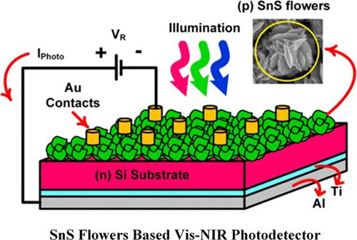
This paper reports a simple, low-cost, and high-performance two-dimensional (2D) nanopetal-assembled three-dimensional (3D) SnS flowers/Si heterojunction-based visible–near-infrared (vis–NIR) photodetector (PD). A modified chemical bath deposition (CBD) method was used to grow a uniform and closely spaced array of SnS flowers on a Si substrate. This type of nanostructure offers a large photoactive area, thus generating a large number of carriers. The high-performance parameters of the fabricated PD (responsivity, 68.21 A/W; external quantum efficiency (EQE), 1.32 × 10⁴%; detectivity, 6.87 × 10¹³ Jones; rise time, 193.91 ms; and fall time, 94.19 ms at 635 nm) are attributed to the heterojunction characteristics resulting from closely spaced nanopetal-assembled SnS flowers on silicon.
期刊介绍:
ACS Applied Electronic Materials is an interdisciplinary journal publishing original research covering all aspects of electronic materials. The journal is devoted to reports of new and original experimental and theoretical research of an applied nature that integrate knowledge in the areas of materials science, engineering, optics, physics, and chemistry into important applications of electronic materials. Sample research topics that span the journal's scope are inorganic, organic, ionic and polymeric materials with properties that include conducting, semiconducting, superconducting, insulating, dielectric, magnetic, optoelectronic, piezoelectric, ferroelectric and thermoelectric.
Indexed/Abstracted:
Web of Science SCIE
Scopus
CAS
INSPEC
Portico

 求助内容:
求助内容: 应助结果提醒方式:


