Research progress and applications of optoelectronic synaptic devices based on 2D materials

Brain-X Pub Date : 2024-10-20 DOI:10.1002/brx2.70004
Yukun Zhao, Linrui Cheng, Rui Xu, Zexin Yu, Jianya Zhang
{"title":"Research progress and applications of optoelectronic synaptic devices based on 2D materials","authors":"Yukun Zhao,&nbsp;Linrui Cheng,&nbsp;Rui Xu,&nbsp;Zexin Yu,&nbsp;Jianya Zhang","doi":"10.1002/brx2.70004","DOIUrl":null,"url":null,"abstract":"<div>\n \n \n <section>\n \n <p>In the natural world, the human brain is the most powerful information processor, using a highly parallel, efficient, fault-tolerant, and reconfigurable neural network. Taking inspiration from this impressive architecture, optoelectronic synaptic devices have gained considerable attention for their ability to process and retain data simultaneously, making them essential components in the upcoming era of neuromorphic computing systems. In recent years, significant progress has been made in the development of optoelectronic neuromorphic synaptic devices using two-dimensional (2D) material heterostructures. This review focuses on the use of 2D materials in creating optoelectronic synaptic devices. It discusses the recent progress made in utilizing 2D material heterostructures in these devices and examines their potential in different areas such as image recognition, neuromorphic wearable electronics, logical operations, and neuromorphic computing systems. Heterostructures made with 2D materials provide a wide range of possibilities as their electronic band structures can be easily tailored to achieve effective optical and electrical modulation. Optoelectronic synaptic devices based on 2D materials simultaneously exhibit two functionalities: detection and memory. Furthermore, these materials have strong interatomic bonding within layers and possess a thickness of only one atomic layer, giving them exceptional flexibility, optical transparency, and mechanical strength. By utilizing 2D materials for solution processing and their ultra-thin profile, the manufacturing of three-terminal synapses becomes cost-effective, simplifying integration processes.</p>\n </section>\n </div>","PeriodicalId":94303,"journal":{"name":"Brain-X","volume":"2 3","pages":""},"PeriodicalIF":0.0000,"publicationDate":"2024-10-20","publicationTypes":"Journal Article","fieldsOfStudy":null,"isOpenAccess":false,"openAccessPdf":"https://onlinelibrary.wiley.com/doi/epdf/10.1002/brx2.70004","citationCount":"0","resultStr":null,"platform":"Semanticscholar","paperid":null,"PeriodicalName":"Brain-X","FirstCategoryId":"1085","ListUrlMain":"https://onlinelibrary.wiley.com/doi/10.1002/brx2.70004","RegionNum":0,"RegionCategory":null,"ArticlePicture":[],"TitleCN":null,"AbstractTextCN":null,"PMCID":null,"EPubDate":"","PubModel":"","JCR":"","JCRName":"","Score":null,"Total":0}
引用次数: 0

Abstract

In the natural world, the human brain is the most powerful information processor, using a highly parallel, efficient, fault-tolerant, and reconfigurable neural network. Taking inspiration from this impressive architecture, optoelectronic synaptic devices have gained considerable attention for their ability to process and retain data simultaneously, making them essential components in the upcoming era of neuromorphic computing systems. In recent years, significant progress has been made in the development of optoelectronic neuromorphic synaptic devices using two-dimensional (2D) material heterostructures. This review focuses on the use of 2D materials in creating optoelectronic synaptic devices. It discusses the recent progress made in utilizing 2D material heterostructures in these devices and examines their potential in different areas such as image recognition, neuromorphic wearable electronics, logical operations, and neuromorphic computing systems. Heterostructures made with 2D materials provide a wide range of possibilities as their electronic band structures can be easily tailored to achieve effective optical and electrical modulation. Optoelectronic synaptic devices based on 2D materials simultaneously exhibit two functionalities: detection and memory. Furthermore, these materials have strong interatomic bonding within layers and possess a thickness of only one atomic layer, giving them exceptional flexibility, optical transparency, and mechanical strength. By utilizing 2D materials for solution processing and their ultra-thin profile, the manufacturing of three-terminal synapses becomes cost-effective, simplifying integration processes.
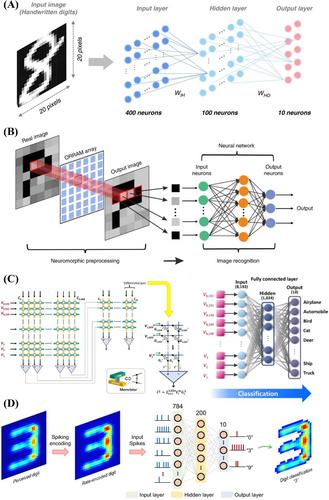
Abstract Image

基于二维材料的光电突触器件的研究进展与应用
在自然界中,人脑是最强大的信息处理器,它使用的是高度并行、高效、容错和可重构的神经网络。从这一令人印象深刻的架构中汲取灵感,光电突触设备因其同时处理和保留数据的能力而备受关注,成为即将到来的神经形态计算系统时代的重要组成部分。近年来,利用二维(2D)材料异质结构开发光电神经形态突触器件取得了重大进展。本综述重点介绍利用二维材料制造光电突触器件的情况。它讨论了在这些器件中利用二维材料异质结构所取得的最新进展,并研究了它们在图像识别、神经形态可穿戴电子设备、逻辑运算和神经形态计算系统等不同领域的潜力。使用二维材料制成的异质结构具有广泛的可能性,因为它们的电子带结构可以轻松定制,以实现有效的光学和电子调制。基于二维材料的光电突触设备同时具有探测和记忆两种功能。此外,这些材料层内原子间结合力强,厚度仅为一个原子层,因此具有优异的柔韧性、光学透明度和机械强度。通过利用二维材料的溶液处理及其超薄外形,三端突触的制造变得具有成本效益,从而简化了集成过程。
本文章由计算机程序翻译,如有差异,请以英文原文为准。
求助全文
约1分钟内获得全文 求助全文
来源期刊
自引率
0.00%
发文量
0
×
引用
GB/T 7714-2015
复制
MLA
复制
APA
复制
导出至
BibTeX EndNote RefMan NoteFirst NoteExpress
×
提示
您的信息不完整,为了账户安全,请先补充。
现在去补充
×
提示
您因"违规操作"
具体请查看互助需知
我知道了
×
提示
确定
请完成安全验证×
copy
已复制链接
快去分享给好友吧!
我知道了
右上角分享
点击右上角分享
0
联系我们:info@booksci.cn Book学术提供免费学术资源搜索服务,方便国内外学者检索中英文文献。致力于提供最便捷和优质的服务体验。 Copyright © 2023 布克学术 All rights reserved.
京ICP备2023020795号-1
ghs 京公网安备 11010802042870号
Book学术文献互助
Book学术文献互助群
群 号:481959085
Book学术官方微信