Organic Light-Emitting Diodes Comprising an Undoped Thermally Activated Delayed Fluorescence Emissive Layer and a Thick Inorganic Perovskite Hole Transport Layer
IF 6.7
1区 物理与天体物理
Q1 MATERIALS SCIENCE, MULTIDISCIPLINARY
引用次数: 0
Abstract
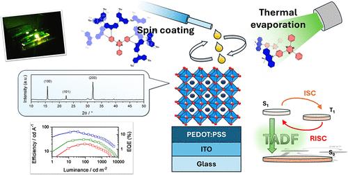
Organic light-emitting diodes (OLEDs) hold potential for next-generation displays and lighting solutions, but current OLED displays rely on the use of scarce metals or fluorescent emitters. Thermally activated delayed fluorescence (TADF) compounds kickstarted a new, promising class of OLEDs as organic TADF emitters do not contain scarce platinoid elements yet remain highly efficient. However, similarly to phosphorescent emitters, their incorporation into devices typically requires complicated doping techniques when vacuum processed. Lowering the mass production costs of high-performing OLEDs using simpler fabrication techniques remains a challenge. Here, we report OLEDs comprising a thermally evaporated CsPbCl3 perovskite transport layer and a TADF-based single-component emitting layer by exploring different approaches to obtain efficient undoped OLEDs, both solution- and vacuum-processed. We first demonstrated the compatibility of the perovskite layer with the solution processing of a TADF dendrimer for host-free, thick emitting layers, with an efficiency of 15 cd A–1 well over a luminance of 1000 cd m–2. Then, we employed a TADF small molecule as the emitter and reduced its layer’s thickness to the subnanometer regime, while the incorporation of the perovskite increased the required total device thickness. The resulting devices showed a low turn-on voltage of 3.3 V, a high luminance of 11 152 cd m–2, and a high efficiency of 67.6 cd A–1, equaling that of 20 times thicker emissive layers. These findings highlight the versatility of using a perovskite as a transport layer and the potential of combining it with an undoped TADF emitting layer for fabricating simple, cost-effective, and efficient OLEDs.
由未掺杂热激活延迟荧光发射层和厚无机 Perovskite 孔传输层组成的有机发光二极管
有机发光二极管(OLED)具有下一代显示器和照明解决方案的潜力,但目前的 OLED 显示器依赖于使用稀缺金属或荧光发射器。热激活延迟荧光(TADF)化合物开创了一种新型、有前途的有机发光二极管,因为有机 TADF 发射器不含稀缺的铂元素,但仍具有很高的效率。然而,与磷光发光体类似,在真空处理时,将它们加入设备中通常需要复杂的掺杂技术。利用更简单的制造技术降低高性能有机发光二极管的量产成本仍然是一项挑战。在此,我们报告了由热蒸发 CsPbCl3 包晶传输层和基于 TADF 的单组分发光层组成的有机发光二极管,通过探索不同的方法来获得高效的溶液和真空处理未掺杂有机发光二极管。我们首先证明了包晶层与 TADF 树枝状聚合物溶液处理的兼容性,从而获得了无宿主、厚的发光层,在 1000 cd m-2 的亮度范围内,发光效率达到 15 cd A-1。然后,我们采用了一种 TADF 小分子作为发光体,并将其层厚度减小到亚纳米级,而包晶石的加入则增加了所需的器件总厚度。结果显示,器件的开启电压低至 3.3 V,亮度高达 11 152 cd m-2,效率高达 67.6 cd A-1,相当于发射层厚度的 20 倍。这些发现凸显了使用包晶石作为传输层的多功能性,以及将其与未掺杂的 TADF 发射层相结合,制造简单、经济、高效的有机发光二极管的潜力。
本文章由计算机程序翻译,如有差异,请以英文原文为准。
求助全文
约1分钟内获得全文
求助全文
来源期刊

ACS Photonics
NANOSCIENCE & NANOTECHNOLOGY-MATERIALS SCIENCE, MULTIDISCIPLINARY
CiteScore
11.90
自引率
5.70%
发文量
438
审稿时长
2.3 months
期刊介绍:
Published as soon as accepted and summarized in monthly issues, ACS Photonics will publish Research Articles, Letters, Perspectives, and Reviews, to encompass the full scope of published research in this field.
 求助内容:
求助内容: 应助结果提醒方式:


