A Unique VO2 Heterojunction-Based Ultrafast Photodetector Configuration for Exceptional Quantum Efficiency and Superior Responsivity
IF 4.3
3区 材料科学
Q1 ENGINEERING, ELECTRICAL & ELECTRONIC
引用次数: 0
Abstract
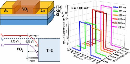
Metal–semiconductor–metal (MSM) photodetectors (PD) are highly versatile and beneficial in a vast array of optical and optoelectronic systems. Although vanadium dioxide (VO2) has a high broadband absorbance, its distinctive electrical and structural features have mostly been utilized for near-infrared (NIR) photodetection. Here, we propose a unique design for a PD using a heterojunction made of VO2/oxygenated-Ti (Ti–O) sandwiched between two Au electrodes. The VO2 film acts as a photon accumulator in this arrangement, and the band bending at the VO2/Ti–O interface helps to separate charges to reduce carrier recombination and inject electrons into the more conductive Ti–O layer. The design completely eliminated all size restrictions of the active layer, regardless of its electrical conductivity, and demonstrated superiority in almost all performance metrics. A remarkable photocurrent density of around 57 μA/cm2 and a rapid response time of 1–2 ms in the presence of visible light was seen at a low bias voltage of 100 mV. The highest detectivity and photocurrent density obtained in our experimental range were 3.2 × 10¹⁰ Jones, and 465 μA/cm2, respectively, using an 800 mV bias voltage and 590 nm light (power density: 76 μW/cm2). For VO2(M)-based MSM type devices, the proposed PD design exhibited the highest responsivity of approximately 2.54 A/W and an exceptional external quantum efficiency (EQE) of around 534%.

基于独特 VO2 异质结的超快光电探测器配置,可实现非凡的量子效率和卓越的响应度
金属-半导体-金属(MSM)光电探测器(PD)用途广泛,可用于各种光学和光电系统。虽然二氧化钒(VO2)具有很高的宽带吸收率,但其独特的电学和结构特征大多被用于近红外(NIR)光电探测。在这里,我们提出了一种独特的光电检测设计,使用夹在两个金电极之间的由二氧化二氧 化物/氧化钛(Ti-O)组成的异质结。在这种布局中,VO2 薄膜起着光子累积器的作用,VO2/Ti-O 接口处的带弯曲有助于分离电荷以减少载流子重组,并将电子注入导电性更强的 Ti-O 层。这种设计完全消除了活性层的所有尺寸限制,无论其导电性如何,并在几乎所有性能指标上都表现出优越性。在 100 mV 的低偏置电压下,光电流密度约为 57 μA/cm2,在可见光下的快速反应时间为 1-2 ms。在我们的实验范围内,使用 800 mV 偏置电压和 590 nm 光(功率密度:76 μW/cm2)获得的最高检测率和光电流密度分别为 3.2 × 10¹⁰ Jones 和 465 μA/cm2。对于基于 VO2(M)的 MSM 型器件,拟议的 PD 设计显示出最高的响应率(约 2.54 A/W )和约 534% 的优异外部量子效率 (EQE)。
本文章由计算机程序翻译,如有差异,请以英文原文为准。
求助全文
约1分钟内获得全文
求助全文
来源期刊

ACS Applied Electronic Materials
Multiple-
CiteScore
7.20
自引率
4.30%
发文量
567
期刊介绍:
ACS Applied Electronic Materials is an interdisciplinary journal publishing original research covering all aspects of electronic materials. The journal is devoted to reports of new and original experimental and theoretical research of an applied nature that integrate knowledge in the areas of materials science, engineering, optics, physics, and chemistry into important applications of electronic materials. Sample research topics that span the journal's scope are inorganic, organic, ionic and polymeric materials with properties that include conducting, semiconducting, superconducting, insulating, dielectric, magnetic, optoelectronic, piezoelectric, ferroelectric and thermoelectric.
Indexed/Abstracted:
Web of Science SCIE
Scopus
CAS
INSPEC
Portico
 求助内容:
求助内容: 应助结果提醒方式:


