Short-Channel Effect Suppression and Footprint Reduction in Double Gate-All-Around Field Effect Transistors and Inverters Based on Two-Dimensional Materials
IF 4.3
3区 材料科学
Q1 ENGINEERING, ELECTRICAL & ELECTRONIC
引用次数: 0
Abstract
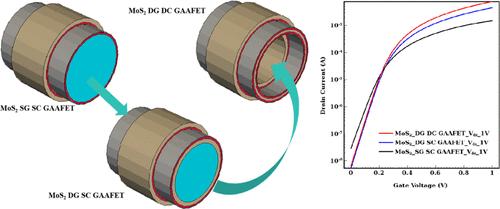
The incessant reduction of transistor dimensions requires new transformations in devices or novel materials to further sustain Moore’s law. From the 5 nm technology node and beyond, the gate-all-around field effect transistor (GAAFET) dominates the semiconductor industry, owing to its ultimate gate electrostatic controllability. Two-dimensional (2D) materials possess the merits of dangling-bond-free surfaces, atomic thicknesses down to sub-1 nm, and high mobility maintenance at sub-1 nm thickness, which are challenges long plaguing traditional three-dimensional (3D) semiconductors. Herein, we devised a double-gated GAAFET (DG GAAFET) based on monolayer MoS2. Compared with a DG GAAFET based on Si with the same footprint, the MoS2 DG GAAFET demonstrates the capability of suppressing short-channel effects out of the regime of the Si DG GAAFET, though a relatively small Ion value, which is attributed to the lower density of states, has been obtained in the monolayer MoS2 DG GAAFET. A single-gated GAAFET based on monolayer MoS2 (MoS2 SG GAAFET) has also been simulated as a control device, which manifests an inferior device performance and degraded short-channel effects compared to those of the MoS2 DG GAAFET, which are revealed by larger SS and a reduced Ion/Ioff ratio. It is verified to be feasible to surge Ion by 84% without short-channel effect degradation via the incorporation of an additional channel, bobbing well for the application of the DG GAAFET device based on 2D materials in high-performance electronics. Besides, a logic inverter based on a double-channeled double-gated GAAFET (DG DC GAAFET) based on WSe2 and MoS2 has been simulated, and a voltage gain of 36 has been obtained under a gate voltage of 2 V. Moreover, an additional degree of freedom can be introduced by adding a SiO2 interlayer, which contributes to the subthreshold voltage matching between a MoS2 n-type transistor and a WSe2 p-type transistor, where a voltage gain of 45 at a gate voltage of 2 V has been obtained. Both the above complementary metal–oxide–semiconductor (CMOS) inverter structures can make full play of the inner areas of the GAA structure, which sheds light on the footprint decrease of inverters, leaving room for more electronics to be crammed into a single chip.
基于二维材料的双栅极全方位场效应晶体管和逆变器中的短沟道效应抑制与占板面积减小
晶体管尺寸的不断缩小要求在器件或新型材料方面进行新的变革,以进一步维持摩尔定律。从 5 纳米技术节点开始,栅极周围场效应晶体管(GAAFET)凭借其极致的栅极静电可控性在半导体行业占据主导地位。二维(2D)材料具有无悬浮键表面、原子厚度低至 1 纳米以下、在 1 纳米以下厚度时仍能保持高迁移率等优点,这些都是长期困扰传统三维(3D)半导体的难题。在此,我们设计了一种基于单层 MoS2 的双栅 GAAFET(DG GAAFET)。与基底面相同的基于硅的 DG GAAFET 相比,MoS2 DG GAAFET 能够抑制硅 DG GAAFET 的短沟道效应,但单层 MoS2 DG GAAFET 的离子值相对较小,这归因于较低的态密度。我们还模拟了一个基于单层 MoS2 的单栅极 GAAFET(MoS2 SG GAAFET)作为控制器件,与 MoS2 DG GAAFET 相比,它的器件性能较差,短沟道效应退化,表现为 SS 较大,Ion/Ioff 比值降低。经过验证,通过加入额外的沟道,可以在不降低短沟道效应的情况下将离子激增 84%,这为基于二维材料的 DG GAAFET 器件在高性能电子器件中的应用提供了良好的条件。此外,还模拟了一种基于 WSe2 和 MoS2 的双通道双栅 GAAFET(DG DC GAAFET)逻辑反相器,在 2 V 栅极电压下获得了 36 的电压增益。此外,通过添加一层二氧化硅(SiO2)夹层,还可以引入额外的自由度,这有助于 MoS2 n 型晶体管和 WSe2 p 型晶体管之间的阈下电压匹配,在栅极电压为 2 V 时可获得 45 的电压增益。上述两种互补金属氧化物半导体(CMOS)逆变器结构都能充分利用 GAA 结构的内部区域,从而减少了逆变器的占地面积,为在单个芯片中容纳更多电子器件留出了空间。
本文章由计算机程序翻译,如有差异,请以英文原文为准。
求助全文
约1分钟内获得全文
求助全文
来源期刊

ACS Applied Electronic Materials
Multiple-
CiteScore
7.20
自引率
4.30%
发文量
567
期刊介绍:
ACS Applied Electronic Materials is an interdisciplinary journal publishing original research covering all aspects of electronic materials. The journal is devoted to reports of new and original experimental and theoretical research of an applied nature that integrate knowledge in the areas of materials science, engineering, optics, physics, and chemistry into important applications of electronic materials. Sample research topics that span the journal's scope are inorganic, organic, ionic and polymeric materials with properties that include conducting, semiconducting, superconducting, insulating, dielectric, magnetic, optoelectronic, piezoelectric, ferroelectric and thermoelectric.
Indexed/Abstracted:
Web of Science SCIE
Scopus
CAS
INSPEC
Portico
 求助内容:
求助内容: 应助结果提醒方式:


