Study on Growth Quality of GaN Deposition on Nanopillar-Patterned Substrates: Microstructure Characterization and Crystalline Quality Optimization
IF 3.2
2区 化学
Q2 CHEMISTRY, MULTIDISCIPLINARY
引用次数: 0
Abstract
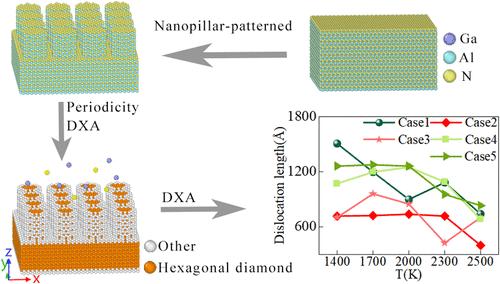
The preparation of gallium nitride (GaN) film materials has significant importance in the semiconductor and thermoelectric sectors, serving as essential core materials for chips, power supply, and communication applications. The production of GaN thin films with reduced defect density has emerged as a significant and continuous subject of research. This work investigated the deposition process of GaN thin films on an aluminum nitride nanopattern substrate via molecular dynamics simulation. A comparison was made between the deposition process on the nanopatterned and unpatterned substrates. Additionally, the impact of the substrate temperature and nanopillar radius on the quality of the thin film was examined. Results demonstrate that the use of a nanopillar pattern on the substrate facilitates the acquisition of the deposited film with a larger number of wurtzite structures and a reduced presence of dislocations. In contrast to the persistent and extensive dislocations formed in the thin films on an unpatterned substrate, the dislocations present in the thin films on a patterned substrate exhibit shorter lengths and more complexity. By appropriately elevating the temperature of the substrate, it is possible to effectively decrease the complexity of the atomic structure and enhance the thin film density. The correlation between the stress and the temperature of the thin film deposited on the patterned substrate is weak. The deformation of nanopillars with a too small radius can cause the deposited atoms to move into the nanovoid, aggravating the irregularity of the thin film surface and the volume of defects. Moreover, the excessive size of the nanopillar at which the surface area of the substrate approaches that of an unpatterned substrate can increase the occurrence of dislocations in the deposited film. This observation implies that the nanovoid ratio inside the nanopillar has a substantial impact on the deposition quality of the thin film. This study focuses on the deposition of GaN films on substrates with nanopatterns at the nanoscale, assesses the impact of nanopatterning degree on the growth quality of film, and acquires data on the temperature range and structural characteristics of high-quality films exhibiting high density and few dislocations.

纳米柱图案基底上氮化镓沉积生长质量研究:显微结构表征和结晶质量优化
氮化镓(GaN)薄膜材料的制备在半导体和热电领域具有重要意义,是芯片、电源和通信应用中不可或缺的核心材料。生产缺陷密度更低的氮化镓薄膜已成为一项重要的持续研究课题。这项工作通过分子动力学模拟研究了氮化铝纳米图案基底上氮化镓薄膜的沉积过程。比较了纳米图案基底和无图案基底上的沉积过程。此外,还研究了基底温度和纳米柱半径对薄膜质量的影响。结果表明,在基底上使用纳米柱图案有利于获得具有更多钨锆石结构和更少位错的沉积薄膜。与在无图案基底上的薄膜中形成的持久而广泛的位错相比,在有图案基底上的薄膜中出现的位错长度更短,复杂性更高。通过适当提高基底的温度,可以有效降低原子结构的复杂性,提高薄膜密度。沉积在图案化基底上的薄膜的应力和温度之间的相关性很弱。半径过小的纳米柱的变形会导致沉积的原子移动到纳米卵形体中,加剧薄膜表面的不规则性和缺陷体积。此外,如果纳米柱的尺寸过大,基底的表面积接近于无图案基底的表面积,则会增加沉积薄膜中位错的发生。这一观察结果表明,纳米柱内部的纳米虚像比对薄膜的沉积质量有很大影响。本研究的重点是在具有纳米级纳米图案的衬底上沉积氮化镓薄膜,评估纳米图案化程度对薄膜生长质量的影响,并获得关于具有高密度和少位错的高质量薄膜的温度范围和结构特征的数据。
本文章由计算机程序翻译,如有差异,请以英文原文为准。
求助全文
约1分钟内获得全文
求助全文
来源期刊

Crystal Growth & Design
化学-材料科学:综合
CiteScore
6.30
自引率
10.50%
发文量
650
审稿时长
1.9 months
期刊介绍:
The aim of Crystal Growth & Design is to stimulate crossfertilization of knowledge among scientists and engineers working in the fields of crystal growth, crystal engineering, and the industrial application of crystalline materials.
Crystal Growth & Design publishes theoretical and experimental studies of the physical, chemical, and biological phenomena and processes related to the design, growth, and application of crystalline materials. Synergistic approaches originating from different disciplines and technologies and integrating the fields of crystal growth, crystal engineering, intermolecular interactions, and industrial application are encouraged.
 求助内容:
求助内容: 应助结果提醒方式:


