High-Efficiency Doping Outcomes in Homoepitaxial β-Ga2O3 Films via Pulsed Si Doping with MOCVD

IF 3.2 2区 化学 Q2 CHEMISTRY, MULTIDISCIPLINARY
Yao Wang, Qian Feng, Wenkai Wu, Yuhong Liu, Yachao Zhang, Jincheng Zhang, Yue Hao
{"title":"High-Efficiency Doping Outcomes in Homoepitaxial β-Ga2O3 Films via Pulsed Si Doping with MOCVD","authors":"Yao Wang, Qian Feng, Wenkai Wu, Yuhong Liu, Yachao Zhang, Jincheng Zhang, Yue Hao","doi":"10.1021/acs.cgd.4c01049","DOIUrl":null,"url":null,"abstract":"Using metal–organic chemical vapor deposition, pulsed Si-doped homoepitaxial gallium oxide (β-Ga<sub>2</sub>O<sub>3</sub>) films were deposited on (010) β-Ga<sub>2</sub>O<sub>3</sub> substrates. The impact of the Si pulse duty cycle on the morphology, structure, and electrical properties of the films was investigated. The full width at half-maximum (fwhm) of the (020) rocking curves for all doped films was less than 55 arcsec, indicating high crystal quality. Employing pulse width modulation of Si doping, as opposed to continuous Si doping, has resulted in a reduction in surface roughness by approximately 2.83 to 9.32 times. Notably, under the conditions of a 0.3 min Si source vent time and a 0.1 min run, an activation ratio of up to 99.1% was achieved, maximizing the electrical performance. This included achieving the lowest resistivity of 0.0042 Ω·cm and an electron mobility of 44.1 cm<sup>2</sup>/(V s) at a carrier concentration of 3.35 × 10<sup>19</sup> cm<sup>–3</sup>. The application of pulsed Si doping provided sufficient diffusion time for Si atoms, enabling effective doping and thereby enhancing the high carrier concentration electrical performance of the films, offering an effective pathway for their use as ohmic contacts in ultrawide-bandgap semiconductor devices.","PeriodicalId":34,"journal":{"name":"Crystal Growth & Design","volume":null,"pages":null},"PeriodicalIF":3.2000,"publicationDate":"2024-09-13","publicationTypes":"Journal Article","fieldsOfStudy":null,"isOpenAccess":false,"openAccessPdf":"","citationCount":"0","resultStr":null,"platform":"Semanticscholar","paperid":null,"PeriodicalName":"Crystal Growth & Design","FirstCategoryId":"92","ListUrlMain":"https://doi.org/10.1021/acs.cgd.4c01049","RegionNum":2,"RegionCategory":"化学","ArticlePicture":[],"TitleCN":null,"AbstractTextCN":null,"PMCID":null,"EPubDate":"","PubModel":"","JCR":"Q2","JCRName":"CHEMISTRY, MULTIDISCIPLINARY","Score":null,"Total":0}
引用次数: 0

Abstract

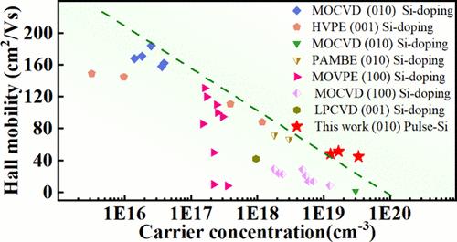
Using metal–organic chemical vapor deposition, pulsed Si-doped homoepitaxial gallium oxide (β-Ga2O3) films were deposited on (010) β-Ga2O3 substrates. The impact of the Si pulse duty cycle on the morphology, structure, and electrical properties of the films was investigated. The full width at half-maximum (fwhm) of the (020) rocking curves for all doped films was less than 55 arcsec, indicating high crystal quality. Employing pulse width modulation of Si doping, as opposed to continuous Si doping, has resulted in a reduction in surface roughness by approximately 2.83 to 9.32 times. Notably, under the conditions of a 0.3 min Si source vent time and a 0.1 min run, an activation ratio of up to 99.1% was achieved, maximizing the electrical performance. This included achieving the lowest resistivity of 0.0042 Ω·cm and an electron mobility of 44.1 cm2/(V s) at a carrier concentration of 3.35 × 1019 cm–3. The application of pulsed Si doping provided sufficient diffusion time for Si atoms, enabling effective doping and thereby enhancing the high carrier concentration electrical performance of the films, offering an effective pathway for their use as ohmic contacts in ultrawide-bandgap semiconductor devices.

Abstract Image

通过脉冲硅掺杂与 MOCVD 在同位β-Ga2O3 薄膜中实现高效掺杂结果
利用金属有机化学气相沉积技术,在 (010) β-Ga2O3 基底上沉积了脉冲掺杂硅的同外延氧化镓 (β-Ga2O3)薄膜。研究了硅脉冲占空比对薄膜形貌、结构和电性能的影响。所有掺杂薄膜的 (020) 摇摆曲线的半最大全宽(fwhm)均小于 55 弧秒,表明晶体质量很高。与连续掺入硅相比,采用脉冲宽度调制掺入硅可将表面粗糙度降低约 2.83 至 9.32 倍。值得注意的是,在硅源通气时间为 0.3 分钟、运行时间为 0.1 分钟的条件下,活化率高达 99.1%,实现了电气性能的最大化。这包括在载流子浓度为 3.35 × 1019 cm-3 时,实现了 0.0042 Ω-cm 的最低电阻率和 44.1 cm2/(V s) 的电子迁移率。脉冲硅掺杂的应用为硅原子提供了充足的扩散时间,实现了有效掺杂,从而提高了薄膜的高载流子浓度电性能,为其在超宽带隙半导体器件中用作欧姆触点提供了有效途径。
本文章由计算机程序翻译,如有差异,请以英文原文为准。
求助全文
约1分钟内获得全文 求助全文
来源期刊
Crystal Growth & Design
Crystal Growth & Design 化学-材料科学:综合
CiteScore
6.30
自引率
10.50%
发文量
650
审稿时长
1.9 months
期刊介绍: The aim of Crystal Growth & Design is to stimulate crossfertilization of knowledge among scientists and engineers working in the fields of crystal growth, crystal engineering, and the industrial application of crystalline materials. Crystal Growth & Design publishes theoretical and experimental studies of the physical, chemical, and biological phenomena and processes related to the design, growth, and application of crystalline materials. Synergistic approaches originating from different disciplines and technologies and integrating the fields of crystal growth, crystal engineering, intermolecular interactions, and industrial application are encouraged.
×
引用
GB/T 7714-2015
复制
MLA
复制
APA
复制
导出至
BibTeX EndNote RefMan NoteFirst NoteExpress
×
提示
您的信息不完整,为了账户安全,请先补充。
现在去补充
×
提示
您因"违规操作"
具体请查看互助需知
我知道了
×
提示
确定
请完成安全验证×
copy
已复制链接
快去分享给好友吧!
我知道了
右上角分享
点击右上角分享
0
联系我们:info@booksci.cn Book学术提供免费学术资源搜索服务,方便国内外学者检索中英文文献。致力于提供最便捷和优质的服务体验。 Copyright © 2023 布克学术 All rights reserved.
京ICP备2023020795号-1
ghs 京公网安备 11010802042870号
Book学术文献互助
Book学术文献互助群
群 号:481959085
Book学术官方微信