Dual-Electrically Configurable MoTe2/In2S3 Phototransistor toward Multifunctional Applications
IF 16
1区 材料科学
Q1 CHEMISTRY, MULTIDISCIPLINARY
引用次数: 0
Abstract
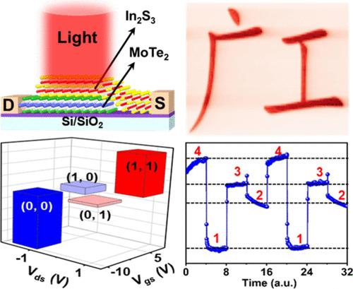
Photodetectors, essential for a wide range of optoelectronic applications in both military and civilian sectors, face challenges in balancing responsivity, detectivity, and response time due to their inherent unidirectional carrier transport mechanism. Multifunctional photodetectors that address these trade-offs are highly sought after for their potential to reduce costs, simplify system design, and surpass Moore’s Law limitations. Herein, we present a multimodal phototransistor based on a 2D MoTe2/In2S3 heterostructure. Through dual electrical modulation employing bias voltage and gate voltage, we engineer the energy band to achieve switchable photoresponse mechanisms between photoconductive and photovoltaic modes. In photoconductive mode, the device exhibits a responsivity of 320 A/W and a specific detectivity of 1.2 × 10¹³ Jones. Meanwhile, in photovoltaic mode, it exhibits a light on/off ratio of 2 × 10⁵ and response speed of 0.68/0.60 ms. These capabilities enable multifunctional applications such as high-resolution imaging across various wavelengths, a conceptual optoelectronic logic gate, and dual-channel optical communication. This work makes an advancement in the development of future multifunctional optoelectronic devices.
面向多功能应用的可配置 MoTe2/In2S3 光电晶体管
光电探测器对于军事和民用领域的各种光电应用都至关重要,但由于其固有的单向载流子传输机制,光电探测器在平衡响应度、检测度和响应时间方面面临挑战。解决这些权衡问题的多功能光电探测器因其具有降低成本、简化系统设计和超越摩尔定律限制的潜力而备受追捧。在此,我们介绍一种基于二维 MoTe2/In2S3 异质结构的多模式光电晶体管。通过使用偏置电压和栅极电压的双电调制,我们设计了能带,实现了光电导模式和光电伏模式之间可切换的光响应机制。在光导模式下,该器件的响应率为 320 A/W,比检测率为 1.2 × 10¹³ Jones。同时,在光电模式下,它的光通/光断比为 2 × 10⁵,响应速度为 0.68/0.60 毫秒。这些性能可实现多功能应用,如不同波长的高分辨率成像、概念光电逻辑门和双通道光通信。这项工作为未来多功能光电器件的开发做出了贡献。
本文章由计算机程序翻译,如有差异,请以英文原文为准。
求助全文
约1分钟内获得全文
求助全文
来源期刊

ACS Nano
工程技术-材料科学:综合
CiteScore
26.00
自引率
4.10%
发文量
1627
审稿时长
1.7 months
期刊介绍:
ACS Nano, published monthly, serves as an international forum for comprehensive articles on nanoscience and nanotechnology research at the intersections of chemistry, biology, materials science, physics, and engineering. The journal fosters communication among scientists in these communities, facilitating collaboration, new research opportunities, and advancements through discoveries. ACS Nano covers synthesis, assembly, characterization, theory, and simulation of nanostructures, nanobiotechnology, nanofabrication, methods and tools for nanoscience and nanotechnology, and self- and directed-assembly. Alongside original research articles, it offers thorough reviews, perspectives on cutting-edge research, and discussions envisioning the future of nanoscience and nanotechnology.
 求助内容:
求助内容: 应助结果提醒方式:


