Tracking Charge Carrier Paths in Freestanding GaN/AlN Nanowires on Si(111)

IF 8.3 2区 材料科学 Q1 MATERIALS SCIENCE, MULTIDISCIPLINARY
Juliane Koch, Patrick Häuser, Peter Kleinschmidt, Werner Prost, Nils Weimann, Thomas Hannappel
{"title":"Tracking Charge Carrier Paths in Freestanding GaN/AlN Nanowires on Si(111)","authors":"Juliane Koch, Patrick Häuser, Peter Kleinschmidt, Werner Prost, Nils Weimann, Thomas Hannappel","doi":"10.1021/acsami.4c10179","DOIUrl":null,"url":null,"abstract":"Functional and abundant substrate materials are relevant for applying all sophisticated semiconductor-based device components such as nanowire arrays. In the case of GaN nanowires grown by metalorganic vapor phase epitaxy, Si(111) substrates are widely used, together with an AlN interlayer to suppress the well-known Ga-based melt-back-etching. However, the AlN interlayer can degrade the interfacial conductivity of the Si(111) substrate. To reveal the possible impact of this interlayer on the overall electrical performance, an advanced analysis of the electrical behavior with suitable spatial resolution is essential. For the electrical investigation of the nanowire-to-substrate junction, we used a four-point probe measurement setup with sufficiently high spatial resolution. The charge separation behavior of the junction is also demonstrated by an electron beam-induced current mode, while the n-GaN nanowire (NW) core exhibits good electrical conductivity. The charge carrier-selective transport at the NW-to-substrate junction can be attributed to different, local material compositions by two main effects: the reduction of Ga adatoms by shadowing of the lower part of the NW structure by the top part during growth, i.e. the protection of the pedestal footprint from Ga adsorption. Our combination of investigation methods provides direct insight into the nanowire-to-substrate junction and leads to a model of the conductivity channels at the nanowire base. This knowledge is crucial for all future GaN bottom-up grown nanowire structure devices on conductive Si(111) substrates.","PeriodicalId":5,"journal":{"name":"ACS Applied Materials & Interfaces","volume":null,"pages":null},"PeriodicalIF":8.3000,"publicationDate":"2024-09-19","publicationTypes":"Journal Article","fieldsOfStudy":null,"isOpenAccess":false,"openAccessPdf":"","citationCount":"0","resultStr":null,"platform":"Semanticscholar","paperid":null,"PeriodicalName":"ACS Applied Materials & Interfaces","FirstCategoryId":"88","ListUrlMain":"https://doi.org/10.1021/acsami.4c10179","RegionNum":2,"RegionCategory":"材料科学","ArticlePicture":[],"TitleCN":null,"AbstractTextCN":null,"PMCID":null,"EPubDate":"","PubModel":"","JCR":"Q1","JCRName":"MATERIALS SCIENCE, MULTIDISCIPLINARY","Score":null,"Total":0}
引用次数: 0

Abstract

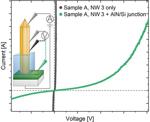
Functional and abundant substrate materials are relevant for applying all sophisticated semiconductor-based device components such as nanowire arrays. In the case of GaN nanowires grown by metalorganic vapor phase epitaxy, Si(111) substrates are widely used, together with an AlN interlayer to suppress the well-known Ga-based melt-back-etching. However, the AlN interlayer can degrade the interfacial conductivity of the Si(111) substrate. To reveal the possible impact of this interlayer on the overall electrical performance, an advanced analysis of the electrical behavior with suitable spatial resolution is essential. For the electrical investigation of the nanowire-to-substrate junction, we used a four-point probe measurement setup with sufficiently high spatial resolution. The charge separation behavior of the junction is also demonstrated by an electron beam-induced current mode, while the n-GaN nanowire (NW) core exhibits good electrical conductivity. The charge carrier-selective transport at the NW-to-substrate junction can be attributed to different, local material compositions by two main effects: the reduction of Ga adatoms by shadowing of the lower part of the NW structure by the top part during growth, i.e. the protection of the pedestal footprint from Ga adsorption. Our combination of investigation methods provides direct insight into the nanowire-to-substrate junction and leads to a model of the conductivity channels at the nanowire base. This knowledge is crucial for all future GaN bottom-up grown nanowire structure devices on conductive Si(111) substrates.
Abstract Image

跟踪硅(111)上独立 GaN/AlN 纳米线中的电荷载流子路径
功能性和丰富的衬底材料与应用纳米线阵列等所有基于半导体的精密设备元件息息相关。在通过金属有机气相外延技术生长氮化镓纳米线的过程中,Si(111)衬底和 AlN 中间膜被广泛使用,以抑制众所周知的镓基熔融背蚀现象。然而,AlN 中间膜会降低硅(111)衬底的界面电导率。为了揭示该中间膜对整体电性能可能产生的影响,必须以适当的空间分辨率对电学行为进行高级分析。为了对纳米线-基底结进行电学研究,我们使用了具有足够高空间分辨率的四点探针测量装置。电子束诱导的电流模式也证明了该结点的电荷分离行为,而 n-GaN 纳米线 (NW) 内核则表现出良好的导电性。氮化镓纳米线与基底交界处的电荷载流子选择性传输可归因于不同的局部材料成分,主要有两种效应:生长过程中氮化镓纳米线结构的下半部分被上半部分遮挡,从而减少了镓吸附原子,即保护基底不被镓吸附。我们将各种研究方法结合起来,可以直接洞察纳米线与基底的交界处,并建立纳米线基底的导电通道模型。这些知识对于未来所有在导电硅(111)衬底上自下而上生长的氮化镓纳米线结构器件至关重要。
本文章由计算机程序翻译,如有差异,请以英文原文为准。
求助全文
约1分钟内获得全文 求助全文
来源期刊
ACS Applied Materials & Interfaces
ACS Applied Materials & Interfaces 工程技术-材料科学:综合
CiteScore
16.00
自引率
6.30%
发文量
4978
审稿时长
1.8 months
期刊介绍: ACS Applied Materials & Interfaces is a leading interdisciplinary journal that brings together chemists, engineers, physicists, and biologists to explore the development and utilization of newly-discovered materials and interfacial processes for specific applications. Our journal has experienced remarkable growth since its establishment in 2009, both in terms of the number of articles published and the impact of the research showcased. We are proud to foster a truly global community, with the majority of published articles originating from outside the United States, reflecting the rapid growth of applied research worldwide.
×
引用
GB/T 7714-2015
复制
MLA
复制
APA
复制
导出至
BibTeX EndNote RefMan NoteFirst NoteExpress
×
提示
您的信息不完整,为了账户安全,请先补充。
现在去补充
×
提示
您因"违规操作"
具体请查看互助需知
我知道了
×
提示
确定
请完成安全验证×
copy
已复制链接
快去分享给好友吧!
我知道了
右上角分享
点击右上角分享
0
联系我们:info@booksci.cn Book学术提供免费学术资源搜索服务,方便国内外学者检索中英文文献。致力于提供最便捷和优质的服务体验。 Copyright © 2023 布克学术 All rights reserved.
京ICP备2023020795号-1
ghs 京公网安备 11010802042870号
Book学术文献互助
Book学术文献互助群
群 号:481959085
Book学术官方微信