Atharva Yeshwant Kulkarni, Gourab Karmakar, Alpa Y. Shah, Harish Donthula, Adish Tyagi* and Rohit Singh Chauhan*,
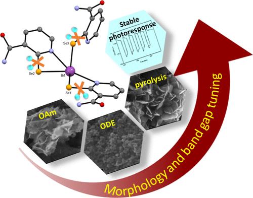
{"title":"Tris(2-selenonicotinamide)bismuth(III) Complex as a Promising Single-Source Precursor for Photoresponsive 2D-Bi2Se3 Nanostructures","authors":"Atharva Yeshwant Kulkarni, Gourab Karmakar, Alpa Y. Shah, Harish Donthula, Adish Tyagi* and Rohit Singh Chauhan*, ","doi":"10.1021/acs.cgd.4c0079810.1021/acs.cgd.4c00798","DOIUrl":null,"url":null,"abstract":"<p >Two-dimensional (2-D) Bi<sub>2</sub>Se<sub>3</sub> nanostructures have emerged as fine candidates due to their appealing performance toward energy conversion and storage applications. In view of this, a simple and economically viable method for their preparation is highly desirable. Herein, we present the synthesis, characterization, and structural elucidation of a new air-stable Bi-nicotinamide selenolate complex: [Bi{SeC<sub>5</sub>H<sub>3</sub>(3-CONH<sub>2</sub>)}<sub>3</sub>] (<b>1</b>). This complex serves as an efficient single-source molecular precursor (SSP) for the facile preparation of phase-pure Bi<sub>2</sub>Se<sub>3</sub> nanostructures. The as-prepared Bi<sub>2</sub>Se<sub>3</sub> nanostructures were characterized using microstructural analyses such as powder X-ray diffraction (PXRD), energy dispersive X-ray spectroscopy (EDS), and electron microscopy techniques to assess their phase purity, elemental composition, crystal structure, and morphology. This study also attempts to understand the effect of reaction conditions on the crystallinity, size, and morphology of nanostructures. The optical band gap of the nanostructures was tuned within the range of 1.9–2.0 eV, which is blue-shifted with respect to the corresponding bulk band gap and is suitable for energy conversion applications. Liquid junction photoelectrochemical cells fabricated from the as-prepared Bi<sub>2</sub>Se<sub>3</sub> nanostructure exhibit good photoresponsivity and decent photostability, which project them as amenable candidates for alternative photon absorber materials.</p>","PeriodicalId":34,"journal":{"name":"Crystal Growth & Design","volume":"24 18","pages":"7570–7579 7570–7579"},"PeriodicalIF":3.4000,"publicationDate":"2024-09-04","publicationTypes":"Journal Article","fieldsOfStudy":null,"isOpenAccess":false,"openAccessPdf":"","citationCount":"0","resultStr":null,"platform":"Semanticscholar","paperid":null,"PeriodicalName":"Crystal Growth & Design","FirstCategoryId":"92","ListUrlMain":"https://pubs.acs.org/doi/10.1021/acs.cgd.4c00798","RegionNum":2,"RegionCategory":"化学","ArticlePicture":[],"TitleCN":null,"AbstractTextCN":null,"PMCID":null,"EPubDate":"","PubModel":"","JCR":"Q2","JCRName":"CHEMISTRY, MULTIDISCIPLINARY","Score":null,"Total":0}
引用次数: 0
Abstract
Two-dimensional (2-D) Bi2Se3 nanostructures have emerged as fine candidates due to their appealing performance toward energy conversion and storage applications. In view of this, a simple and economically viable method for their preparation is highly desirable. Herein, we present the synthesis, characterization, and structural elucidation of a new air-stable Bi-nicotinamide selenolate complex: [Bi{SeC5H3(3-CONH2)}3] (1). This complex serves as an efficient single-source molecular precursor (SSP) for the facile preparation of phase-pure Bi2Se3 nanostructures. The as-prepared Bi2Se3 nanostructures were characterized using microstructural analyses such as powder X-ray diffraction (PXRD), energy dispersive X-ray spectroscopy (EDS), and electron microscopy techniques to assess their phase purity, elemental composition, crystal structure, and morphology. This study also attempts to understand the effect of reaction conditions on the crystallinity, size, and morphology of nanostructures. The optical band gap of the nanostructures was tuned within the range of 1.9–2.0 eV, which is blue-shifted with respect to the corresponding bulk band gap and is suitable for energy conversion applications. Liquid junction photoelectrochemical cells fabricated from the as-prepared Bi2Se3 nanostructure exhibit good photoresponsivity and decent photostability, which project them as amenable candidates for alternative photon absorber materials.
期刊介绍:
The aim of Crystal Growth & Design is to stimulate crossfertilization of knowledge among scientists and engineers working in the fields of crystal growth, crystal engineering, and the industrial application of crystalline materials.
Crystal Growth & Design publishes theoretical and experimental studies of the physical, chemical, and biological phenomena and processes related to the design, growth, and application of crystalline materials. Synergistic approaches originating from different disciplines and technologies and integrating the fields of crystal growth, crystal engineering, intermolecular interactions, and industrial application are encouraged.

 求助内容:
求助内容: 应助结果提醒方式:


