Magnesium niobate as a high-κ gate dielectric for two-dimensional electronics
IF 33.7
1区 工程技术
Q1 ENGINEERING, ELECTRICAL & ELECTRONIC
引用次数: 0
Abstract
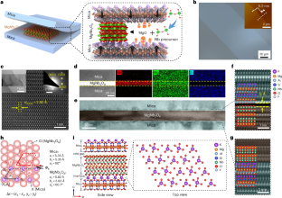
Integrated circuits based on two-dimensional semiconductors require ultrathin gate insulators that can provide high interface quality and dielectric reliability, minimized electrically active traps and efficient gate controllability. However, existing two-dimensional insulators do not provide a good trade-off in terms of bandgap, breakdown strength, dielectric constant, leakage current and bias temperature stability. Here, we show that single crystals of magnesium niobate (MgNb2O6) can be obtained through a buffer-controlled epitaxial growth process on a mica substrate. The atomically thin MgNb2O6 crystals have a wide bandgap (around 5.0 eV), high dielectric constant (around 20), large breakdown voltage (around 16 MV cm−1) and good thermal reliability. The MgNb2O6 can form a van der Waals interface with monolayer molybdenum disulfide (MoS2) with an extremely low density of trap states. MoS2 field-effect transistors with MgNb2O6 gate dielectrics exhibit a hysteresis under 0.9 mV (MV cm−1)−1, a subthreshold swing of 62 mV dec−1, an on/off current ratio of up to 4 × 10⁷ and high electrical reliability at 500 K. The excellent electrostatic controllability of MgNb2O6 allowed us to create graphene-contacted transistors and inverter circuits with a channel length of 50 nm. A high-κ dielectric ceramic, magnesium niobate, can be epitaxially grown on a mica substrate and then transferred to form the gate dielectric in molybdenum disulfide transistors, providing van der Waals interfaces and high robustness to temperature and voltage.


铌酸镁作为二维电子学的高κ栅极电介质
基于二维半导体的集成电路需要超薄栅极绝缘体,以提供高界面质量和介电可靠性、最小电活性阱和高效栅极可控性。然而,现有的二维绝缘体在带隙、击穿强度、介电常数、泄漏电流和偏置温度稳定性等方面并不能很好地实现折衷。在这里,我们展示了在云母衬底上通过缓冲控制外延生长工艺获得的铌酸镁单晶体(MgNb2O6)。原子级薄 MgNb2O6 晶体具有宽带隙(约 5.0 eV)、高介电常数(约 20)、大击穿电压(约 16 MV cm-1)和良好的热可靠性。MgNb2O6 能与单层二硫化钼(MoS2)形成范德华界面,陷阱态密度极低。带有 MgNb2O6 栅极电介质的 MoS2 场效应晶体管在 500 K 时的磁滞低于 0.9 mV (MV cm-1)-1,阈下摆幅为 62 mV dec-1,导通/关断电流比高达 4 × 10⁷,并且具有很高的电气可靠性。MgNb2O6 极佳的静电可控性使我们能够制造出沟道长度为 50 nm 的石墨烯接触晶体管和逆变器电路。
本文章由计算机程序翻译,如有差异,请以英文原文为准。
求助全文
约1分钟内获得全文
求助全文
来源期刊

Nature Electronics
Engineering-Electrical and Electronic Engineering
CiteScore
47.50
自引率
2.30%
发文量
159
期刊介绍:
Nature Electronics is a comprehensive journal that publishes both fundamental and applied research in the field of electronics. It encompasses a wide range of topics, including the study of new phenomena and devices, the design and construction of electronic circuits, and the practical applications of electronics. In addition, the journal explores the commercial and industrial aspects of electronics research.
The primary focus of Nature Electronics is on the development of technology and its potential impact on society. The journal incorporates the contributions of scientists, engineers, and industry professionals, offering a platform for their research findings. Moreover, Nature Electronics provides insightful commentary, thorough reviews, and analysis of the key issues that shape the field, as well as the technologies that are reshaping society.
Like all journals within the prestigious Nature brand, Nature Electronics upholds the highest standards of quality. It maintains a dedicated team of professional editors and follows a fair and rigorous peer-review process. The journal also ensures impeccable copy-editing and production, enabling swift publication. Additionally, Nature Electronics prides itself on its editorial independence, ensuring unbiased and impartial reporting.
In summary, Nature Electronics is a leading journal that publishes cutting-edge research in electronics. With its multidisciplinary approach and commitment to excellence, the journal serves as a valuable resource for scientists, engineers, and industry professionals seeking to stay at the forefront of advancements in the field.
 求助内容:
求助内容: 应助结果提醒方式:


