Photolithography-Free, Solution-Processable Perovskite Electrodes for High-Performance Organic Transistors
IF 9.6
1区 材料科学
Q1 CHEMISTRY, MULTIDISCIPLINARY
引用次数: 0
Abstract
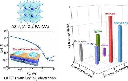
Solution-processable electrodes are promising for next-generation electronics due to their simplicity, cost-effectiveness, and potential for large-area fabrication. However, current solution-processable electrodes based on conductive polymers, carbon-based compounds, and metal nanowires face challenges related to stability, patterning, and production scalability. Here we introduce a novel approach using 3D tin halide perovskites (THPs) combined with a photolithography-free solution patterning technique to fabricate solution-processed electrodes. We demonstrate the preparation of highly conductive CsSnI3 films (234.9 S cm–1) and the fabrication of patterned 35 × 35 perovskite electrode arrays on a 4-in. silicon wafer. These electrodes, used as source/drain electrodes in organic transistors, resulted in devices showing high uniformity and stability. This electrode fabrication strategy is also applicable to other 3D THPs like FASnI3 and MASnI3, showcasing versatility for diverse applications. The results highlight the feasibility and advantages of using 3D THPs as solution-processable electrodes, providing a new material system for the advancement of solution-processed electronics.

用于高性能有机晶体管的免光刻、可溶液加工的 Perovskite 电极
溶液可加工电极因其简便性、成本效益和大面积制造的潜力,在下一代电子技术中大有可为。然而,目前基于导电聚合物、碳基化合物和金属纳米线的溶液可加工电极面临着稳定性、图案化和生产可扩展性方面的挑战。在这里,我们介绍了一种新方法,利用三维卤化锡包荧光体(THPs)结合免光刻溶液图案化技术来制造溶液加工电极。我们展示了高导电性 CsSnI3 薄膜(234.9 S cm-1)的制备过程,以及在 4 英寸硅晶片上制作 35 × 35 包晶体图案化电极阵列的过程。这些电极在有机晶体管中用作源极/漏极,其器件显示出高度的一致性和稳定性。这种电极制造策略也适用于其他三维 THP,如 FASnI3 和 MASnI3,展示了其在各种应用中的多功能性。研究结果凸显了使用三维 THPs 作为溶液加工电极的可行性和优势,为溶液加工电子学的发展提供了一种新的材料系统。
本文章由计算机程序翻译,如有差异,请以英文原文为准。
求助全文
约1分钟内获得全文
求助全文
来源期刊

Nano Letters
工程技术-材料科学:综合
CiteScore
16.80
自引率
2.80%
发文量
1182
审稿时长
1.4 months
期刊介绍:
Nano Letters serves as a dynamic platform for promptly disseminating original results in fundamental, applied, and emerging research across all facets of nanoscience and nanotechnology. A pivotal criterion for inclusion within Nano Letters is the convergence of at least two different areas or disciplines, ensuring a rich interdisciplinary scope. The journal is dedicated to fostering exploration in diverse areas, including:
- Experimental and theoretical findings on physical, chemical, and biological phenomena at the nanoscale
- Synthesis, characterization, and processing of organic, inorganic, polymer, and hybrid nanomaterials through physical, chemical, and biological methodologies
- Modeling and simulation of synthetic, assembly, and interaction processes
- Realization of integrated nanostructures and nano-engineered devices exhibiting advanced performance
- Applications of nanoscale materials in living and environmental systems
Nano Letters is committed to advancing and showcasing groundbreaking research that intersects various domains, fostering innovation and collaboration in the ever-evolving field of nanoscience and nanotechnology.
 求助内容:
求助内容: 应助结果提醒方式:


