Controlled Fabrication of Native Ultra‐Thin Amorphous Gallium Oxide From 2D Gallium Sulfide for Emerging Electronic Applications

IF 4.3 3区 材料科学 Q2 CHEMISTRY, MULTIDISCIPLINARY
AbdulAziz AlMutairi, Aferdita Xhameni, Xuyun Guo, Irina Chircă, Valeria Nicolosi, Stephan Hofmann, Antonio Lombardo
{"title":"Controlled Fabrication of Native Ultra‐Thin Amorphous Gallium Oxide From 2D Gallium Sulfide for Emerging Electronic Applications","authors":"AbdulAziz AlMutairi, Aferdita Xhameni, Xuyun Guo, Irina Chircă, Valeria Nicolosi, Stephan Hofmann, Antonio Lombardo","doi":"10.1002/admi.202400481","DOIUrl":null,"url":null,"abstract":"Oxidation of 2D layered materials has proven advantageous in creating oxide/2D material heterostructures, opening the door for a new paradigm of low‐power electronic devices. Gallium (II) sulfide (β‐GaS), a hexagonal phase group III monochalcogenide, is a wide bandgap semiconductor with a bandgap exceeding 3 eV in single and few‐layer form. Its oxide, gallium oxide (Ga<jats:sub>2</jats:sub>O<jats:sub>3</jats:sub>), combines a large bandgap (4.4–5.3 eV) with a high dielectric constant (≈10). Despite the technological potential of both materials, controlled oxidation of atomically‐thin β‐GaS remains under‐explored. This study focuses on the controlled oxidation of β‐GaS using oxygen plasma treatment, addressing a significant gap in existing research. The results demonstrate the ability to form ultrathin native oxide (GaS<jats:sub>x</jats:sub>O<jats:sub>y</jats:sub>), 4 nm in thickness, upon exposure to 10 W of O<jats:sub>2</jats:sub>, resulting in a GaS<jats:sub>x</jats:sub>O<jats:sub>y</jats:sub>/GaS heterostructure where the GaS layer beneath remains intact. By integrating such structures between metal electrodes and applying electric stresses as voltage ramps or pulses, their use for resistive random‐access memory (ReRAM) is investigated. The ultrathin nature of the produced oxide enables low operation power with energy use as low as 0.22 nJ per operation while maintaining endurance and retention of 350 cycles and 10<jats:sup>4</jats:sup> s, respectively. These results show the significant potential of the oxidation‐based GaS<jats:sub>x</jats:sub>O<jats:sub>y</jats:sub>/GaS heterostructure for electronic applications and, in particular, low‐power memory devices.","PeriodicalId":115,"journal":{"name":"Advanced Materials Interfaces","volume":"9 1","pages":""},"PeriodicalIF":4.3000,"publicationDate":"2024-08-26","publicationTypes":"Journal Article","fieldsOfStudy":null,"isOpenAccess":false,"openAccessPdf":"","citationCount":"0","resultStr":null,"platform":"Semanticscholar","paperid":null,"PeriodicalName":"Advanced Materials Interfaces","FirstCategoryId":"88","ListUrlMain":"https://doi.org/10.1002/admi.202400481","RegionNum":3,"RegionCategory":"材料科学","ArticlePicture":[],"TitleCN":null,"AbstractTextCN":null,"PMCID":null,"EPubDate":"","PubModel":"","JCR":"Q2","JCRName":"CHEMISTRY, MULTIDISCIPLINARY","Score":null,"Total":0}
引用次数: 0

Abstract

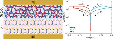
Oxidation of 2D layered materials has proven advantageous in creating oxide/2D material heterostructures, opening the door for a new paradigm of low‐power electronic devices. Gallium (II) sulfide (β‐GaS), a hexagonal phase group III monochalcogenide, is a wide bandgap semiconductor with a bandgap exceeding 3 eV in single and few‐layer form. Its oxide, gallium oxide (Ga2O3), combines a large bandgap (4.4–5.3 eV) with a high dielectric constant (≈10). Despite the technological potential of both materials, controlled oxidation of atomically‐thin β‐GaS remains under‐explored. This study focuses on the controlled oxidation of β‐GaS using oxygen plasma treatment, addressing a significant gap in existing research. The results demonstrate the ability to form ultrathin native oxide (GaSxOy), 4 nm in thickness, upon exposure to 10 W of O2, resulting in a GaSxOy/GaS heterostructure where the GaS layer beneath remains intact. By integrating such structures between metal electrodes and applying electric stresses as voltage ramps or pulses, their use for resistive random‐access memory (ReRAM) is investigated. The ultrathin nature of the produced oxide enables low operation power with energy use as low as 0.22 nJ per operation while maintaining endurance and retention of 350 cycles and 104 s, respectively. These results show the significant potential of the oxidation‐based GaSxOy/GaS heterostructure for electronic applications and, in particular, low‐power memory devices.

Abstract Image

从二维硫化镓受控制备原生超薄非晶氧化镓,用于新兴电子应用
事实证明,二维层状材料的氧化在创建氧化物/二维材料异质结构方面具有优势,为低功耗电子设备的新模式打开了大门。硫化镓(II)(β-GaS)是一种六方相 III 族单质,是一种宽带隙半导体,其单层和少层带隙超过 3 eV。其氧化物氧化镓(Ga2O3)兼具大带隙(4.4-5.3 eV)和高介电常数(≈10)。尽管这两种材料都具有技术潜力,但原子级薄 β-GaS的受控氧化仍未得到充分探索。本研究的重点是利用氧等离子体处理技术对β-GaS进行受控氧化,以弥补现有研究中的重大空白。研究结果表明,在暴露于 10 W 氧气时,能够形成厚度为 4 nm 的超薄原生氧化物 (GaSxOy),从而形成 GaSxOy/GaS 异质结构,其下的 GaS 层保持完整。通过将这种结构集成在金属电极之间,并施加电压斜坡或脉冲电应力,研究了它们在电阻式随机存取存储器(ReRAM)中的应用。生成的氧化物具有超薄特性,可实现低操作功耗,每次操作的能耗低至 0.22 nJ,同时还能分别保持 350 次循环和 104 秒的耐久性和保持时间。这些结果表明,基于氧化的 GaSxOy/GaS 异质结构在电子应用,特别是低功耗存储器件方面具有巨大潜力。
本文章由计算机程序翻译,如有差异,请以英文原文为准。
求助全文
约1分钟内获得全文 求助全文
来源期刊
Advanced Materials Interfaces
Advanced Materials Interfaces CHEMISTRY, MULTIDISCIPLINARY-MATERIALS SCIENCE, MULTIDISCIPLINARY
CiteScore
8.40
自引率
5.60%
发文量
1174
审稿时长
1.3 months
期刊介绍: Advanced Materials Interfaces publishes top-level research on interface technologies and effects. Considering any interface formed between solids, liquids, and gases, the journal ensures an interdisciplinary blend of physics, chemistry, materials science, and life sciences. Advanced Materials Interfaces was launched in 2014 and received an Impact Factor of 4.834 in 2018. The scope of Advanced Materials Interfaces is dedicated to interfaces and surfaces that play an essential role in virtually all materials and devices. Physics, chemistry, materials science and life sciences blend to encourage new, cross-pollinating ideas, which will drive forward our understanding of the processes at the interface. Advanced Materials Interfaces covers all topics in interface-related research: Oil / water separation, Applications of nanostructured materials, 2D materials and heterostructures, Surfaces and interfaces in organic electronic devices, Catalysis and membranes, Self-assembly and nanopatterned surfaces, Composite and coating materials, Biointerfaces for technical and medical applications. Advanced Materials Interfaces provides a forum for topics on surface and interface science with a wide choice of formats: Reviews, Full Papers, and Communications, as well as Progress Reports and Research News.
×
引用
GB/T 7714-2015
复制
MLA
复制
APA
复制
导出至
BibTeX EndNote RefMan NoteFirst NoteExpress
×
提示
您的信息不完整,为了账户安全,请先补充。
现在去补充
×
提示
您因"违规操作"
具体请查看互助需知
我知道了
×
提示
确定
请完成安全验证×
copy
已复制链接
快去分享给好友吧!
我知道了
右上角分享
点击右上角分享
0
联系我们:info@booksci.cn Book学术提供免费学术资源搜索服务,方便国内外学者检索中英文文献。致力于提供最便捷和优质的服务体验。 Copyright © 2023 布克学术 All rights reserved.
京ICP备2023020795号-1
ghs 京公网安备 11010802042870号
Book学术文献互助
Book学术文献互助群
群 号:481959085
Book学术官方微信