Remote epitaxy and freestanding wide bandgap semiconductor membrane technology

Minseong Park, Takuji Maekawa, Kyungwook Hwang, Jim Cable, Watanabe Noriyuki, Kisik Choi, Young-Kyun Noh, Youngtek Oh, Yongmin Baek, Kyusang Lee
{"title":"Remote epitaxy and freestanding wide bandgap semiconductor membrane technology","authors":"Minseong Park, Takuji Maekawa, Kyungwook Hwang, Jim Cable, Watanabe Noriyuki, Kisik Choi, Young-Kyun Noh, Youngtek Oh, Yongmin Baek, Kyusang Lee","doi":"10.1038/s44287-024-00091-0","DOIUrl":null,"url":null,"abstract":"The emergence of artificial intelligence, big data processing, electrical vehicle technologies and so on necessitates a new approach to address the scaling, power efficiency and performance challenges of silicon (Si)-based technology beyond Moore’s law. As a complementary technology, wide bandgap semiconductors, including GaN and SiC, have attracted great attention owing to their unique features of high carrier mobility and high breakdown voltages. However, there are still limitations for widespread applications of wide bandgap semiconductors including scalability, high production cost and thermal management. To overcome these barriers, remote epitaxy and 2D layer transfer technology have been introduced and are in the process of being industrialized to produce single-crystalline semiconductor-based freestanding membranes. In this Perspective, we present the status and challenges for manufacturing GaN and SiC membranes based on remote epitaxy technology that offers significant advantages via wafer reuse and high-quality freestanding epilayer production. We also discuss how industrialization of advanced membrane technology can benefit numerous applications, including heterogeneously integrated circuits, power and radiofrequency systems. This Perspective discusses the status and challenges of remote epitaxy technology towards industrialization of wide bandgap semiconductors for the future electronics.","PeriodicalId":501701,"journal":{"name":"Nature Reviews Electrical Engineering","volume":"1 10","pages":"680-689"},"PeriodicalIF":0.0000,"publicationDate":"2024-09-12","publicationTypes":"Journal Article","fieldsOfStudy":null,"isOpenAccess":false,"openAccessPdf":"","citationCount":"0","resultStr":null,"platform":"Semanticscholar","paperid":null,"PeriodicalName":"Nature Reviews Electrical Engineering","FirstCategoryId":"1085","ListUrlMain":"https://www.nature.com/articles/s44287-024-00091-0","RegionNum":0,"RegionCategory":null,"ArticlePicture":[],"TitleCN":null,"AbstractTextCN":null,"PMCID":null,"EPubDate":"","PubModel":"","JCR":"","JCRName":"","Score":null,"Total":0}
引用次数: 0

Abstract

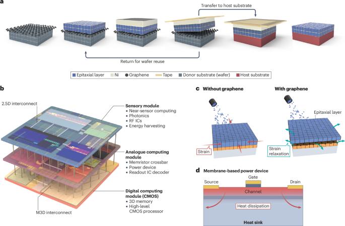
The emergence of artificial intelligence, big data processing, electrical vehicle technologies and so on necessitates a new approach to address the scaling, power efficiency and performance challenges of silicon (Si)-based technology beyond Moore’s law. As a complementary technology, wide bandgap semiconductors, including GaN and SiC, have attracted great attention owing to their unique features of high carrier mobility and high breakdown voltages. However, there are still limitations for widespread applications of wide bandgap semiconductors including scalability, high production cost and thermal management. To overcome these barriers, remote epitaxy and 2D layer transfer technology have been introduced and are in the process of being industrialized to produce single-crystalline semiconductor-based freestanding membranes. In this Perspective, we present the status and challenges for manufacturing GaN and SiC membranes based on remote epitaxy technology that offers significant advantages via wafer reuse and high-quality freestanding epilayer production. We also discuss how industrialization of advanced membrane technology can benefit numerous applications, including heterogeneously integrated circuits, power and radiofrequency systems. This Perspective discusses the status and challenges of remote epitaxy technology towards industrialization of wide bandgap semiconductors for the future electronics.

Abstract Image

Abstract Image

远程外延和独立宽带隙半导体膜技术
人工智能、大数据处理、电动汽车技术等的出现,要求我们采用新的方法来解决硅(Si)技术在摩尔定律之后的扩展、能效和性能挑战。作为一种补充技术,包括氮化镓和碳化硅在内的宽带隙半导体因其独特的高载流子迁移率和高击穿电压特性而备受关注。然而,宽带隙半导体的广泛应用仍受到一些限制,包括可扩展性、高生产成本和热管理。为了克服这些障碍,我们引入了远程外延和二维层转移技术,并正在将其产业化,以生产基于单晶半导体的独立薄膜。在本《视角》中,我们介绍了基于远程外延技术生产氮化镓和碳化硅膜的现状和挑战,该技术通过晶圆重复使用和高质量独立外延层生产具有显著优势。我们还讨论了先进膜技术的产业化如何惠及众多应用,包括异质集成电路、电源和射频系统。
本文章由计算机程序翻译,如有差异,请以英文原文为准。
求助全文
约1分钟内获得全文 求助全文
来源期刊
自引率
0.00%
发文量
0
×
引用
GB/T 7714-2015
复制
MLA
复制
APA
复制
导出至
BibTeX EndNote RefMan NoteFirst NoteExpress
×
提示
您的信息不完整,为了账户安全,请先补充。
现在去补充
×
提示
您因"违规操作"
具体请查看互助需知
我知道了
×
提示
确定
请完成安全验证×
copy
已复制链接
快去分享给好友吧!
我知道了
右上角分享
点击右上角分享
0
联系我们:info@booksci.cn Book学术提供免费学术资源搜索服务,方便国内外学者检索中英文文献。致力于提供最便捷和优质的服务体验。 Copyright © 2023 布克学术 All rights reserved.
京ICP备2023020795号-1
ghs 京公网安备 11010802042870号
Book学术文献互助
Book学术文献互助群
群 号:481959085
Book学术官方微信