Investigating multipurpose reddish-orange emitting vanadate-based nanomaterials activated by Sm(III) for use in latent fingerprinting and photophysical applications
IF 2.8 4区 工程技术Q2 ENGINEERING, ELECTRICAL & ELECTRONIC
{"title":"Investigating multipurpose reddish-orange emitting vanadate-based nanomaterials activated by Sm(III) for use in latent fingerprinting and photophysical applications","authors":"Neeraj Sehrawat, Poonam Devi, Hina Dalal, Diksha Solanki, Ojas Garg, Mukesh Kumar, Sapana Garg","doi":"10.1007/s10854-024-13408-4","DOIUrl":null,"url":null,"abstract":"<p>Here, we report the synthesis of Sm<sup>3+</sup>- activated Ca<sub>8</sub>ZnBi(VO<sub>4</sub>)<sub>7</sub> nanophosphors using the easy, economic, and time-saving urea-aided solution combustion method. The fabricated powder samples that were annealed at 900 °C were examined for their structural, morphological, and optical characteristics. By recording the X-ray diffraction pattern, R3c (161), the space group and the trigonal phase of synthesized phosphor, was verified. Using X-ray energy-dispersive spectroscopy and scanning electron microscopy, the morphology and elemental composition of the phosphors were examined. Using a transmission electron microscope (TEM), the fabricated nanophosphor particle size was examined. A TEM image demonstrates the occurrence of uneven particle agglomeration in the nanoscale range. The synthesized phosphors’ excitation, emission spectra were captured to examine their photoluminescence (PL) behavior. We observed characteristic reddish-orange Sm<sup>3+</sup> PL emission when the produced Ca<sub>8</sub>ZnBi (VO<sub>4</sub>)<sub>7</sub> phosphors material was exposed to UV light at 408 nm, this corresponded to the transition <sup>4</sup>G<sub>5/2</sub> → <sup>6</sup>H<sub>7/2</sub>, at 605 nm, respectively. Dexter’s theory and the Inokuti–Hirayama (I–H) model were used to confirm that the energy migration among neighbor ions is found to be responsible for concentration quenching and 5 mol % is found to be the optimal concentration of dopant ion. Using the diffuse reflectance (DR) spectrum, the Eg (bandgap) values for Ca<sub>8</sub>ZnBi(VO<sub>4</sub>)<sub>7</sub> (3.18 eV) and Ca<sub>8</sub>ZnBi<sub>0.95</sub>Sm<sub>0.05</sub>(VO<sub>4</sub>)<sub>7</sub> (3.15 eV) were determined. In addition, a detailed evaluation was conducted on the quantum efficiency (64.74 %), radiative lifetime (0.6329 ms), and color coordinates (0.6522,0.3476). These astounding outcomes demonstrated the synthesized nanomaterials suitability for creating wLEDs, inherent fingerprinting, and other photophysical claims.</p>","PeriodicalId":646,"journal":{"name":"Journal of Materials Science: Materials in Electronics","volume":null,"pages":null},"PeriodicalIF":2.8000,"publicationDate":"2024-09-04","publicationTypes":"Journal Article","fieldsOfStudy":null,"isOpenAccess":false,"openAccessPdf":"","citationCount":"0","resultStr":null,"platform":"Semanticscholar","paperid":null,"PeriodicalName":"Journal of Materials Science: Materials in Electronics","FirstCategoryId":"5","ListUrlMain":"https://doi.org/10.1007/s10854-024-13408-4","RegionNum":4,"RegionCategory":"工程技术","ArticlePicture":[],"TitleCN":null,"AbstractTextCN":null,"PMCID":null,"EPubDate":"","PubModel":"","JCR":"Q2","JCRName":"ENGINEERING, ELECTRICAL & ELECTRONIC","Score":null,"Total":0}
引用次数: 0
Abstract
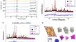
Here, we report the synthesis of Sm3+- activated Ca8ZnBi(VO4)7 nanophosphors using the easy, economic, and time-saving urea-aided solution combustion method. The fabricated powder samples that were annealed at 900 °C were examined for their structural, morphological, and optical characteristics. By recording the X-ray diffraction pattern, R3c (161), the space group and the trigonal phase of synthesized phosphor, was verified. Using X-ray energy-dispersive spectroscopy and scanning electron microscopy, the morphology and elemental composition of the phosphors were examined. Using a transmission electron microscope (TEM), the fabricated nanophosphor particle size was examined. A TEM image demonstrates the occurrence of uneven particle agglomeration in the nanoscale range. The synthesized phosphors’ excitation, emission spectra were captured to examine their photoluminescence (PL) behavior. We observed characteristic reddish-orange Sm3+ PL emission when the produced Ca8ZnBi (VO4)7 phosphors material was exposed to UV light at 408 nm, this corresponded to the transition 4G5/2 → 6H7/2, at 605 nm, respectively. Dexter’s theory and the Inokuti–Hirayama (I–H) model were used to confirm that the energy migration among neighbor ions is found to be responsible for concentration quenching and 5 mol % is found to be the optimal concentration of dopant ion. Using the diffuse reflectance (DR) spectrum, the Eg (bandgap) values for Ca8ZnBi(VO4)7 (3.18 eV) and Ca8ZnBi0.95Sm0.05(VO4)7 (3.15 eV) were determined. In addition, a detailed evaluation was conducted on the quantum efficiency (64.74 %), radiative lifetime (0.6329 ms), and color coordinates (0.6522,0.3476). These astounding outcomes demonstrated the synthesized nanomaterials suitability for creating wLEDs, inherent fingerprinting, and other photophysical claims.
期刊介绍:
The Journal of Materials Science: Materials in Electronics is an established refereed companion to the Journal of Materials Science. It publishes papers on materials and their applications in modern electronics, covering the ground between fundamental science, such as semiconductor physics, and work concerned specifically with applications. It explores the growth and preparation of new materials, as well as their processing, fabrication, bonding and encapsulation, together with the reliability, failure analysis, quality assurance and characterization related to the whole range of applications in electronics. The Journal presents papers in newly developing fields such as low dimensional structures and devices, optoelectronics including III-V compounds, glasses and linear/non-linear crystal materials and lasers, high Tc superconductors, conducting polymers, thick film materials and new contact technologies, as well as the established electronics device and circuit materials.

 求助内容:
求助内容: 应助结果提醒方式:


