Hiral M. Mistry, M. P. Deshpande, Anilkumar B. Hirpara, Nidhishree M. Suchak, Sunil H. Chaki, Sandip V. Bhatt
{"title":"A photonic insight of NiO–GO nanocomposites synthesized by Adhatoda vasica extracts","authors":"Hiral M. Mistry, M. P. Deshpande, Anilkumar B. Hirpara, Nidhishree M. Suchak, Sunil H. Chaki, Sandip V. Bhatt","doi":"10.1007/s10854-024-13452-0","DOIUrl":null,"url":null,"abstract":"<p>The low-cost, simple, and environmentally friendly green synthesis of nickel oxide nanoparticles (NiO) and related hybrids through plant extracts has gained a lot of interest nowadays. In this work, a one-step green synthesis of hybrid Nickel Oxide-Graphene oxide nanocomposites (NiO–GO NCs) utilizing an Adhatoda vasica extract was undertaken. Numerous analytical techniques, such as EDX, XPS, FESEM, HRTEM, XRD, Raman spectroscopy, FTIR, and UV–visible spectroscopy, were employed to assess the formation of NiO on GO. The study explored the light responsiveness of NiO–GO NCs by obtaining current–voltage (I–V) measurements under visible light exposure. The synthesized NiO–GO NCs exhibited remarkable and extensive sensitivity to light over a variety of wavelengths. Furthermore, responsivity and detectivity were maximum at 480 nm (9.83 mA/W, 2.53<b> × </b>10<sup><b>9</b></sup> Jones), followed by 7.54 mA/W, 1.94<b> × </b>10<sup><b>9</b></sup> Jones, and 3.98 mA/W, 1.02<b> × </b>10<sup><b>9</b></sup> Jones, at 520 and 670 nm respectively. At 480 nm, with a biasing voltage as low as 1 nV, we got a responsivity of 6.91 µA/W and a detectivity of 5.15<b> × </b>10<sup><b>7</b></sup> Jones. The photodetector showed a positive photoresponse between 5–30 V and a negative one between 1–100 nanovolts. This controllable approach for switching between positive and negative photoconductivity adds an extra functionality to conventional optoelectronic devices.</p>","PeriodicalId":646,"journal":{"name":"Journal of Materials Science: Materials in Electronics","volume":null,"pages":null},"PeriodicalIF":2.8000,"publicationDate":"2024-09-05","publicationTypes":"Journal Article","fieldsOfStudy":null,"isOpenAccess":false,"openAccessPdf":"","citationCount":"0","resultStr":null,"platform":"Semanticscholar","paperid":null,"PeriodicalName":"Journal of Materials Science: Materials in Electronics","FirstCategoryId":"5","ListUrlMain":"https://doi.org/10.1007/s10854-024-13452-0","RegionNum":4,"RegionCategory":"工程技术","ArticlePicture":[],"TitleCN":null,"AbstractTextCN":null,"PMCID":null,"EPubDate":"","PubModel":"","JCR":"Q2","JCRName":"ENGINEERING, ELECTRICAL & ELECTRONIC","Score":null,"Total":0}
引用次数: 0
Abstract
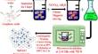
The low-cost, simple, and environmentally friendly green synthesis of nickel oxide nanoparticles (NiO) and related hybrids through plant extracts has gained a lot of interest nowadays. In this work, a one-step green synthesis of hybrid Nickel Oxide-Graphene oxide nanocomposites (NiO–GO NCs) utilizing an Adhatoda vasica extract was undertaken. Numerous analytical techniques, such as EDX, XPS, FESEM, HRTEM, XRD, Raman spectroscopy, FTIR, and UV–visible spectroscopy, were employed to assess the formation of NiO on GO. The study explored the light responsiveness of NiO–GO NCs by obtaining current–voltage (I–V) measurements under visible light exposure. The synthesized NiO–GO NCs exhibited remarkable and extensive sensitivity to light over a variety of wavelengths. Furthermore, responsivity and detectivity were maximum at 480 nm (9.83 mA/W, 2.53 × 10⁹ Jones), followed by 7.54 mA/W, 1.94 × 10⁹ Jones, and 3.98 mA/W, 1.02 × 10⁹ Jones, at 520 and 670 nm respectively. At 480 nm, with a biasing voltage as low as 1 nV, we got a responsivity of 6.91 µA/W and a detectivity of 5.15 × 10⁷ Jones. The photodetector showed a positive photoresponse between 5–30 V and a negative one between 1–100 nanovolts. This controllable approach for switching between positive and negative photoconductivity adds an extra functionality to conventional optoelectronic devices.
期刊介绍:
The Journal of Materials Science: Materials in Electronics is an established refereed companion to the Journal of Materials Science. It publishes papers on materials and their applications in modern electronics, covering the ground between fundamental science, such as semiconductor physics, and work concerned specifically with applications. It explores the growth and preparation of new materials, as well as their processing, fabrication, bonding and encapsulation, together with the reliability, failure analysis, quality assurance and characterization related to the whole range of applications in electronics. The Journal presents papers in newly developing fields such as low dimensional structures and devices, optoelectronics including III-V compounds, glasses and linear/non-linear crystal materials and lasers, high Tc superconductors, conducting polymers, thick film materials and new contact technologies, as well as the established electronics device and circuit materials.

 求助内容:
求助内容: 应助结果提醒方式:


