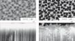
Formation of Channel Silicon to Create Filter Layers
IF 0.6
4区 物理与天体物理
Q4 PHYSICS, CONDENSED MATTER
引用次数: 0
Abstract
The features of the formation of porous layers on substrates of low doped silicon of и-type conductivity by anodic etching using illumination are considered. The formation of microporous silicon layer on the walls of macropores was found. It is shown that the illumination modes strongly influence the morphological parameters of the obtained layers. After exposure to alkali, macroporous layers with pore diameters up to 550 nm were obtained, which can be used to create filter layers.
形成通道硅以创建滤波器层
摘要 研究了利用光照在低掺杂硅基底上通过阳极蚀刻形成多孔层的特点。研究发现在大孔壁上形成了微孔硅层。研究表明,照明模式对所获得层的形态参数有很大影响。暴露于碱液后,获得了孔径达 550 nm 的大孔层,可用于制造过滤层。
本文章由计算机程序翻译,如有差异,请以英文原文为准。
求助全文
约1分钟内获得全文
求助全文
来源期刊
Semiconductors
物理-物理:凝聚态物理
CiteScore
1.50
自引率
28.60%
发文量
131
审稿时长
3-6 weeks
期刊介绍:
Publishes the most important work in semiconductor research in the countries of the former Soviet Union. Covers semiconductor theory, transport phenomena in semiconductors, optics, magnetooptics, and electrooptics of semiconductors, semiconductor lasers and semiconductor surface physics. The journal features an extensive book review section.
 求助内容:
求助内容: 应助结果提醒方式:


