High-performance single-crystalline In2O3 field effect transistor toward three-dimensional large-scale integration circuits

IF 7.5 Q1 MATERIALS SCIENCE, MULTIDISCIPLINARY
Shunpei Yamazaki, Fumito Isaka, Toshikazu Ohno, Yuji Egi, Sachiaki Tezuka, Motomu Kurata, Hiromi Sawai, Ryosuke Motoyoshi, Etsuko Asano, Satoru Saito, Tatsuya Onuki, Takanori Matsuzaki, Michio Tajima
{"title":"High-performance single-crystalline In2O3 field effect transistor toward three-dimensional large-scale integration circuits","authors":"Shunpei Yamazaki, Fumito Isaka, Toshikazu Ohno, Yuji Egi, Sachiaki Tezuka, Motomu Kurata, Hiromi Sawai, Ryosuke Motoyoshi, Etsuko Asano, Satoru Saito, Tatsuya Onuki, Takanori Matsuzaki, Michio Tajima","doi":"10.1038/s43246-024-00625-x","DOIUrl":null,"url":null,"abstract":"Formation of a single crystalline oxide semiconductor on an insulating film as a channel material capable of three-dimensional (3D) stacking would enable 3D very-large-scale integration circuits. This study presents a technique for forming single-crystalline In2O3 having no grain boundaries in a channel formation region on an insulating film using the (001) plane of c-axis-aligned crystalline indium gallium zinc oxide as a seed. Vertical field-effect transistors using the single-crystalline In2O3 had an off-state current of 10−21 A μm−1 and electrical characteristics were improved compared with those using non-single-crystalline In2O3: the subthreshold slope was improved from 95.7 to 86.7 mV dec.−1, the threshold voltage showing normally-off characteristics (0.10 V) was obtained, the threshold voltage standard deviation was improved from 0.11 to 0.05 V, the on-state current was improved from 22.5 to 28.8 μA, and a 17-digit on/off ratio was obtained at 27 °C. Three-dimensional stacking of single-crystalline oxide semiconductors on insulating films is key to large-scale integration of electronic circuits. Here, a technique is reported for single-crystalline In2O3 formation over an insulting film with no grain boundaries, achieving high processing speed and low power consumption.","PeriodicalId":10589,"journal":{"name":"Communications Materials","volume":" ","pages":"1-11"},"PeriodicalIF":7.5000,"publicationDate":"2024-09-11","publicationTypes":"Journal Article","fieldsOfStudy":null,"isOpenAccess":false,"openAccessPdf":"https://www.nature.com/articles/s43246-024-00625-x.pdf","citationCount":"0","resultStr":null,"platform":"Semanticscholar","paperid":null,"PeriodicalName":"Communications Materials","FirstCategoryId":"1085","ListUrlMain":"https://www.nature.com/articles/s43246-024-00625-x","RegionNum":0,"RegionCategory":null,"ArticlePicture":[],"TitleCN":null,"AbstractTextCN":null,"PMCID":null,"EPubDate":"","PubModel":"","JCR":"Q1","JCRName":"MATERIALS SCIENCE, MULTIDISCIPLINARY","Score":null,"Total":0}
引用次数: 0

Abstract

Formation of a single crystalline oxide semiconductor on an insulating film as a channel material capable of three-dimensional (3D) stacking would enable 3D very-large-scale integration circuits. This study presents a technique for forming single-crystalline In2O3 having no grain boundaries in a channel formation region on an insulating film using the (001) plane of c-axis-aligned crystalline indium gallium zinc oxide as a seed. Vertical field-effect transistors using the single-crystalline In2O3 had an off-state current of 10−21 A μm−1 and electrical characteristics were improved compared with those using non-single-crystalline In2O3: the subthreshold slope was improved from 95.7 to 86.7 mV dec.−1, the threshold voltage showing normally-off characteristics (0.10 V) was obtained, the threshold voltage standard deviation was improved from 0.11 to 0.05 V, the on-state current was improved from 22.5 to 28.8 μA, and a 17-digit on/off ratio was obtained at 27 °C. Three-dimensional stacking of single-crystalline oxide semiconductors on insulating films is key to large-scale integration of electronic circuits. Here, a technique is reported for single-crystalline In2O3 formation over an insulting film with no grain boundaries, achieving high processing speed and low power consumption.
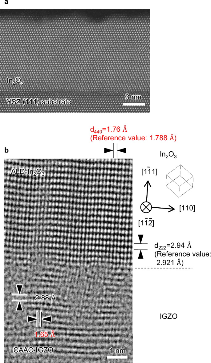
Abstract Image

Abstract Image

面向三维大规模集成电路的高性能单晶 In2O3 场效应晶体管
在绝缘薄膜上形成单晶氧化物半导体作为能够进行三维(3D)堆叠的沟道材料,可实现三维超大规模集成电路。本研究提出了一种在绝缘薄膜上的沟道形成区域形成没有晶界的单晶 In2O3 的技术,该技术以 c 轴对齐的晶体氧化铟镓锌的 (001) 平面为种子。与使用非单晶 In2O3 的晶体管相比,使用单晶 In2O3 的垂直场效应晶体管的离态电流为 10-21 A μm-1,电气特性也有所改善:阈下斜率从 95.7 mV dec.-阈值电压显示正常关断特性(0.10 V),阈值电压标准偏差从 0.11 V 减小到 0.05 V,导通电流从 22.5 μA 减小到 28.8 μA,并且在 27 °C 时获得了 17 位数的导通/关断比。
本文章由计算机程序翻译,如有差异,请以英文原文为准。
求助全文
约1分钟内获得全文 求助全文
来源期刊
Communications Materials
Communications Materials MATERIALS SCIENCE, MULTIDISCIPLINARY-
CiteScore
12.10
自引率
1.30%
发文量
85
审稿时长
17 weeks
期刊介绍: Communications Materials, a selective open access journal within Nature Portfolio, is dedicated to publishing top-tier research, reviews, and commentary across all facets of materials science. The journal showcases significant advancements in specialized research areas, encompassing both fundamental and applied studies. Serving as an open access option for materials sciences, Communications Materials applies less stringent criteria for impact and significance compared to Nature-branded journals, including Nature Communications.
×
引用
GB/T 7714-2015
复制
MLA
复制
APA
复制
导出至
BibTeX EndNote RefMan NoteFirst NoteExpress
×
提示
您的信息不完整,为了账户安全,请先补充。
现在去补充
×
提示
您因"违规操作"
具体请查看互助需知
我知道了
×
提示
确定
请完成安全验证×
copy
已复制链接
快去分享给好友吧!
我知道了
右上角分享
点击右上角分享
0
联系我们:info@booksci.cn Book学术提供免费学术资源搜索服务,方便国内外学者检索中英文文献。致力于提供最便捷和优质的服务体验。 Copyright © 2023 布克学术 All rights reserved.
京ICP备2023020795号-1
ghs 京公网安备 11010802042870号
Book学术文献互助
Book学术文献互助群
群 号:481959085
Book学术官方微信