Optimization of Growth Temperature and V/III Ratio toward High-Quality Si-Doped Aluminum Nitride Thin Films on Sapphire
IF 3.2
2区 化学
Q2 CHEMISTRY, MULTIDISCIPLINARY
引用次数: 0
Abstract
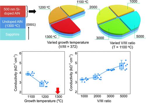
Ultrawide-band-gap aluminum nitride (AlN) boasts high breakdown field strength, superior thermal conductivity, and exceptional stability, making it ideal for deep ultraviolet optoelectronics, radio frequency, and power devices. To date, the epitaxial growth of high-quality doped AlN via MOCVD has primarily been on AlN or SiC single-crystal substrates to reduce dislocation densities. However, the limited size and high cost of these single-crystal substrates necessitate the exploration of alternative substrates to enhance commercial viability. This study demonstrates and analyzes the epitaxial growth modes and conductivity modulation mechanisms of AlN:Si on a cost-effective sapphire substrate. By adjusting MOCVD epitaxial parameters: growth temperature and V/III ratio, we controlled the impact of compensating defects (CN and VAl) on conductivity, achieving conductivity enhancements of 26 and 41%, respectively. Our research validates the feasibility of obtaining AlN:Si with enhanced electrical performance and crystal quality on sapphire substrates. It represents a significant step toward the development of high-power, high-efficiency AlN electronic devices.
优化生长温度和 V/III 比率,在蓝宝石上形成高质量的掺硅氮化铝薄膜
超宽带隙氮化铝(AlN)具有高击穿场强、优异的热导率和超强的稳定性,是深紫外光电子器件、射频器件和功率器件的理想选择。迄今为止,通过 MOCVD 外延生长高质量掺杂氮化铝主要是在氮化铝或碳化硅单晶衬底上进行的,以降低位错密度。然而,这些单晶衬底尺寸有限且成本高昂,因此有必要探索替代衬底,以提高商业可行性。本研究展示并分析了 AlN:Si 在具有成本效益的蓝宝石衬底上的外延生长模式和电导率调制机制。通过调整 MOCVD 外延参数:生长温度和 V/III 比率,我们控制了补偿缺陷(CN 和 VAl)对电导率的影响,使电导率分别提高了 26% 和 41%。我们的研究验证了在蓝宝石衬底上获得电性能和晶体质量更高的 AlN:Si 的可行性。这是向开发大功率、高效 AlN 电子器件迈出的重要一步。
本文章由计算机程序翻译,如有差异,请以英文原文为准。
求助全文
约1分钟内获得全文
求助全文
来源期刊
Crystal Growth & Design
化学-材料科学:综合
CiteScore
6.30
自引率
10.50%
发文量
650
审稿时长
1.9 months
期刊介绍:
The aim of Crystal Growth & Design is to stimulate crossfertilization of knowledge among scientists and engineers working in the fields of crystal growth, crystal engineering, and the industrial application of crystalline materials.
Crystal Growth & Design publishes theoretical and experimental studies of the physical, chemical, and biological phenomena and processes related to the design, growth, and application of crystalline materials. Synergistic approaches originating from different disciplines and technologies and integrating the fields of crystal growth, crystal engineering, intermolecular interactions, and industrial application are encouraged.
 求助内容:
求助内容: 应助结果提醒方式:


