Md. Shah Alam, Rawdad Nawer Warda, Omi Akter, Dipta Kumar Das
{"title":"Performance Impact of Lead-Free CsSn0.5Ge0.5I3 Based Perovskite Solar Cells with HTL-Free Incorporation","authors":"Md. Shah Alam, Rawdad Nawer Warda, Omi Akter, Dipta Kumar Das","doi":"10.1002/gch2.202400141","DOIUrl":null,"url":null,"abstract":"<p>Lead-containing halide perovskites show promise for solar energy but pose ecological and health risks. To address these, researchers are exploring inorganic binary metal perovskites. This study proposes an eco-friendly, durable hole transport layer (HTL)-free design of CsSn<sub>0.5</sub>Ge<sub>0.5</sub>I<sub>3</sub> with high power conversion efficiency (PCE). Using the SCAPS-1D simulator, we assessed the efficiency of an HTL-free planar heterojunction, while the Density Functional Theory (DFT)-based CASTEP simulator evaluated the optical properties of CsSn<sub>0.5</sub>Ge<sub>0.5</sub>I<sub>3</sub> in an orthorhombic structure. Key findings highlight enhanced performance under 100 Wm<sup>−2</sup> AM 1.5G illumination by optimizing absorber layer thickness to 800 nm and reducing defect densities in both the perovskite absorber layer and interfaces to 1 × 10<sup>14</sup> cm<sup>−3</sup>.Additonally, the effects of different electron transport materials (ETMs), optimization of electron transport layer (ETL) thickness (30-50 nm), and back contact design improvements were examined. The simulation's results included an increase over the highest values reported in the literature: an open circuit voltage (Voc) of 1.06 V, a short circuit current density (Jsc) of 28.52 mA/cm<sup>2</sup>, a fill factor (FF) of 86.57%, and a PCE of 26.18% for the FTO/Zn<sub>0.875</sub>Mg<sub>0.125</sub>O/CsSn<sub>0.5</sub>Ge<sub>0.5</sub>I<sub>3</sub>/Se perovskite solar cell (PSC). This research provides theoretical insights for developing high-efficiency power modules without HTLs with significant industrial and research potential.</p>","PeriodicalId":12646,"journal":{"name":"Global Challenges","volume":"8 10","pages":""},"PeriodicalIF":4.4000,"publicationDate":"2024-08-28","publicationTypes":"Journal Article","fieldsOfStudy":null,"isOpenAccess":false,"openAccessPdf":"https://onlinelibrary.wiley.com/doi/epdf/10.1002/gch2.202400141","citationCount":"0","resultStr":null,"platform":"Semanticscholar","paperid":null,"PeriodicalName":"Global Challenges","FirstCategoryId":"103","ListUrlMain":"https://onlinelibrary.wiley.com/doi/10.1002/gch2.202400141","RegionNum":4,"RegionCategory":"综合性期刊","ArticlePicture":[],"TitleCN":null,"AbstractTextCN":null,"PMCID":null,"EPubDate":"","PubModel":"","JCR":"Q1","JCRName":"MULTIDISCIPLINARY SCIENCES","Score":null,"Total":0}
引用次数: 0
Abstract
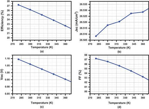
Lead-containing halide perovskites show promise for solar energy but pose ecological and health risks. To address these, researchers are exploring inorganic binary metal perovskites. This study proposes an eco-friendly, durable hole transport layer (HTL)-free design of CsSn0.5Ge0.5I3 with high power conversion efficiency (PCE). Using the SCAPS-1D simulator, we assessed the efficiency of an HTL-free planar heterojunction, while the Density Functional Theory (DFT)-based CASTEP simulator evaluated the optical properties of CsSn0.5Ge0.5I3 in an orthorhombic structure. Key findings highlight enhanced performance under 100 Wm−2 AM 1.5G illumination by optimizing absorber layer thickness to 800 nm and reducing defect densities in both the perovskite absorber layer and interfaces to 1 × 1014 cm−3.Additonally, the effects of different electron transport materials (ETMs), optimization of electron transport layer (ETL) thickness (30-50 nm), and back contact design improvements were examined. The simulation's results included an increase over the highest values reported in the literature: an open circuit voltage (Voc) of 1.06 V, a short circuit current density (Jsc) of 28.52 mA/cm2, a fill factor (FF) of 86.57%, and a PCE of 26.18% for the FTO/Zn0.875Mg0.125O/CsSn0.5Ge0.5I3/Se perovskite solar cell (PSC). This research provides theoretical insights for developing high-efficiency power modules without HTLs with significant industrial and research potential.
 求助内容:
求助内容: 应助结果提醒方式:


