{"title":"Suppressing the vdW Gap-Induced Tunneling Barrier by Constructing Interfacial Covalent Bonds in 2D Metal–Semiconductor Contacts","authors":"Wenchao Shan, Anqi Shi, Zhengyang Xin, Xiuyun Zhang, Bing Wang, Yongtao Li, Xianghong Niu","doi":"10.1002/adfm.202412773","DOIUrl":null,"url":null,"abstract":"<p>2D metal and semiconductor materials provide a promising solution to realize Ohmic contacts by suppressing the strong Fermi level pinning (FLP) effect due to without dangling bonds. However, the 2D metal-semiconductor Van der Waals (vdW) interfaces induce an inevitable tunnel barrier, significantly restraining the injection of charge carriers into the conduction channel. Herein, by replacing the vdW bond with the covalent bond in interfaces, the Ohmic and tunneling-barrier-inhibition contacts are realized simultaneously based on the 2D XSi<sub>2</sub>N<sub>4</sub> (X = Cr, Hf, Mo, Ti, V, Zr) semiconductor and the 2D Mxene metal family. Taking 60 2D Mxene-XSi<sub>2</sub>N<sub>4</sub> contacts as examples, although the vdW-type contacts exhibit Ohmic contacts, the tunneling probability (P<sub>TB</sub>) can be as low as 0.4%, while the P<sub>TB</sub> can increase to 88.09% by removing the Mxene terminations at the adjacent interface to form the covalent bond. The weak FLP and Ohmic contacts are retained at covalent bond interfaces since the outlying Si─N sublayer protects the band-edge electronic states of XSi<sub>2</sub>N<sub>4</sub> semiconductors. This work provides a straightforward strategy for advancing high-performance and energy-efficient 2D electronic nanodevices.</p>","PeriodicalId":112,"journal":{"name":"Advanced Functional Materials","volume":"35 2","pages":""},"PeriodicalIF":18.5000,"publicationDate":"2024-09-12","publicationTypes":"Journal Article","fieldsOfStudy":null,"isOpenAccess":false,"openAccessPdf":"","citationCount":"0","resultStr":null,"platform":"Semanticscholar","paperid":null,"PeriodicalName":"Advanced Functional Materials","FirstCategoryId":"88","ListUrlMain":"https://onlinelibrary.wiley.com/doi/10.1002/adfm.202412773","RegionNum":1,"RegionCategory":"材料科学","ArticlePicture":[],"TitleCN":null,"AbstractTextCN":null,"PMCID":null,"EPubDate":"","PubModel":"","JCR":"Q1","JCRName":"CHEMISTRY, MULTIDISCIPLINARY","Score":null,"Total":0}
引用次数: 0
Abstract
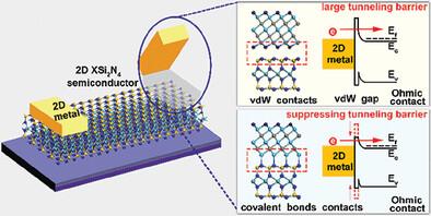
2D metal and semiconductor materials provide a promising solution to realize Ohmic contacts by suppressing the strong Fermi level pinning (FLP) effect due to without dangling bonds. However, the 2D metal-semiconductor Van der Waals (vdW) interfaces induce an inevitable tunnel barrier, significantly restraining the injection of charge carriers into the conduction channel. Herein, by replacing the vdW bond with the covalent bond in interfaces, the Ohmic and tunneling-barrier-inhibition contacts are realized simultaneously based on the 2D XSi2N4 (X = Cr, Hf, Mo, Ti, V, Zr) semiconductor and the 2D Mxene metal family. Taking 60 2D Mxene-XSi2N4 contacts as examples, although the vdW-type contacts exhibit Ohmic contacts, the tunneling probability (PTB) can be as low as 0.4%, while the PTB can increase to 88.09% by removing the Mxene terminations at the adjacent interface to form the covalent bond. The weak FLP and Ohmic contacts are retained at covalent bond interfaces since the outlying Si─N sublayer protects the band-edge electronic states of XSi2N4 semiconductors. This work provides a straightforward strategy for advancing high-performance and energy-efficient 2D electronic nanodevices.
期刊介绍:
Firmly established as a top-tier materials science journal, Advanced Functional Materials reports breakthrough research in all aspects of materials science, including nanotechnology, chemistry, physics, and biology every week.
Advanced Functional Materials is known for its rapid and fair peer review, quality content, and high impact, making it the first choice of the international materials science community.
 求助内容:
求助内容: 应助结果提醒方式:


