Eike Icking, David Emmerich, Kenji Watanabe, Takashi Taniguchi, Bernd Beschoten, Max C Lemme, Joachim Knoch, Christoph Stampfer
{"title":"Ultrasteep Slope Cryogenic FETs Based on Bilayer Graphene.","authors":"Eike Icking, David Emmerich, Kenji Watanabe, Takashi Taniguchi, Bernd Beschoten, Max C Lemme, Joachim Knoch, Christoph Stampfer","doi":"10.1021/acs.nanolett.4c02463","DOIUrl":null,"url":null,"abstract":"<p><p>Cryogenic field-effect transistors (FETs) offer great potential for applications, the most notable example being classical control electronics for quantum information processors. For the latter, on-chip FETs with low power consumption are crucial. This requires operating voltages in the millivolt range, which are only achievable in devices with ultrasteep subthreshold slopes. However, in conventional cryogenic metal-oxide-semiconductor (MOS)FETs based on bulk material, the experimentally achieved inverse subthreshold slopes saturate around a few mV/dec due to disorder and charged defects at the MOS interface. FETs based on two-dimensional materials offer a promising alternative. Here, we show that FETs based on Bernal stacked bilayer graphene encapsulated in hexagonal boron nitride and graphite gates exhibit inverse subthreshold slopes of down to 250 μV/dec at 0.1 K, approaching the Boltzmann limit. This result indicates an effective suppression of band tailing in van der Waals heterostructures without bulk interfaces, leading to superior device performance at cryogenic temperature.</p>","PeriodicalId":53,"journal":{"name":"Nano Letters","volume":null,"pages":null},"PeriodicalIF":9.6000,"publicationDate":"2024-09-18","publicationTypes":"Journal Article","fieldsOfStudy":null,"isOpenAccess":false,"openAccessPdf":"","citationCount":"0","resultStr":null,"platform":"Semanticscholar","paperid":null,"PeriodicalName":"Nano Letters","FirstCategoryId":"88","ListUrlMain":"https://doi.org/10.1021/acs.nanolett.4c02463","RegionNum":1,"RegionCategory":"材料科学","ArticlePicture":[],"TitleCN":null,"AbstractTextCN":null,"PMCID":null,"EPubDate":"2024/9/4 0:00:00","PubModel":"Epub","JCR":"Q1","JCRName":"CHEMISTRY, MULTIDISCIPLINARY","Score":null,"Total":0}
引用次数: 0
Abstract
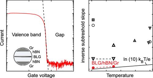
Cryogenic field-effect transistors (FETs) offer great potential for applications, the most notable example being classical control electronics for quantum information processors. For the latter, on-chip FETs with low power consumption are crucial. This requires operating voltages in the millivolt range, which are only achievable in devices with ultrasteep subthreshold slopes. However, in conventional cryogenic metal-oxide-semiconductor (MOS)FETs based on bulk material, the experimentally achieved inverse subthreshold slopes saturate around a few mV/dec due to disorder and charged defects at the MOS interface. FETs based on two-dimensional materials offer a promising alternative. Here, we show that FETs based on Bernal stacked bilayer graphene encapsulated in hexagonal boron nitride and graphite gates exhibit inverse subthreshold slopes of down to 250 μV/dec at 0.1 K, approaching the Boltzmann limit. This result indicates an effective suppression of band tailing in van der Waals heterostructures without bulk interfaces, leading to superior device performance at cryogenic temperature.
低温场效应晶体管(FET)具有巨大的应用潜力,最显著的例子就是量子信息处理器的经典控制电子器件。对于后者,低功耗片上场效应晶体管至关重要。这就需要毫伏级的工作电压,而这只有具有超深亚阈值斜率的器件才能实现。然而,在基于块状材料的传统低温金属氧化物半导体(MOS)场效应晶体管中,由于 MOS 界面的无序和带电缺陷,实验实现的反向亚阈值斜率在几 mV/dec 左右就会饱和。基于二维材料的场效应晶体管提供了一种很有前景的替代方案。在这里,我们展示了基于封装在六方氮化硼和石墨栅极中的贝纳尔堆叠双层石墨烯的场效应晶体管,其在 0.1 K 时的反向次阈值斜率低至 250 μV/dec,接近玻尔兹曼极限。这一结果表明,在没有体界面的范德华异质结构中,能有效抑制带尾,从而在低温条件下实现卓越的器件性能。
期刊介绍:
Nano Letters serves as a dynamic platform for promptly disseminating original results in fundamental, applied, and emerging research across all facets of nanoscience and nanotechnology. A pivotal criterion for inclusion within Nano Letters is the convergence of at least two different areas or disciplines, ensuring a rich interdisciplinary scope. The journal is dedicated to fostering exploration in diverse areas, including:
- Experimental and theoretical findings on physical, chemical, and biological phenomena at the nanoscale
- Synthesis, characterization, and processing of organic, inorganic, polymer, and hybrid nanomaterials through physical, chemical, and biological methodologies
- Modeling and simulation of synthetic, assembly, and interaction processes
- Realization of integrated nanostructures and nano-engineered devices exhibiting advanced performance
- Applications of nanoscale materials in living and environmental systems
Nano Letters is committed to advancing and showcasing groundbreaking research that intersects various domains, fostering innovation and collaboration in the ever-evolving field of nanoscience and nanotechnology.

 求助内容:
求助内容: 应助结果提醒方式:


