Low-loss and compact arbitrary-order silicon mode converter based on hybrid shape optimization

IF 6.5 2区 物理与天体物理 Q1 MATERIALS SCIENCE, MULTIDISCIPLINARY
Junpeng Liao, Dongmei Huang, Yegang Lu, Yan Li, Ye Tian
{"title":"Low-loss and compact arbitrary-order silicon mode converter based on hybrid shape optimization","authors":"Junpeng Liao, Dongmei Huang, Yegang Lu, Yan Li, Ye Tian","doi":"10.1515/nanoph-2024-0301","DOIUrl":null,"url":null,"abstract":"Mode converters (MCs) play an essential role in mode-division multiplexing (MDM) systems. Numerous schemes have been developed on the silicon-on-insulator (SOI) platform, yet most of them focus solely on the conversion of fundamental mode to one or two specific higher-order modes. In this study, we introduce a hybrid shape optimization (HSO) method that combines particle swarm optimization (PSO) with adjoint methods to optimize the shape of the S-bend waveguide, facilitating the design of arbitrary-order MCs featuring compactness and high performance. Our approach was validated by designing a series of 13 μm-long MCs, enabling efficient conversion between various TE modes, ranging from TE<jats:sub>0</jats:sub> to TE<jats:sub>3</jats:sub>. These devices can be fabricated in a single lithography step and exhibit robust fabrication tolerances. Experiment results indicate that these converters achieve low insertion losses under 1 dB and crosstalks below −15 dB across bandwidths of 80 nm (TE<jats:sub>0</jats:sub>–TE<jats:sub>1</jats:sub>), 62 nm (TE<jats:sub>0</jats:sub>–TE<jats:sub>2</jats:sub>), 70 nm (TE<jats:sub>0</jats:sub>–TE<jats:sub>3</jats:sub>), 80 nm (TE<jats:sub>1</jats:sub>–TE<jats:sub>2</jats:sub>), 55 nm (TE<jats:sub>1</jats:sub>–TE<jats:sub>3</jats:sub>), and 75 nm (TE<jats:sub>2</jats:sub>–TE<jats:sub>3</jats:sub>). This advancement paves the way for flexible mode conversion, significantly enhancing the versatility of on-chip MDM technologies.","PeriodicalId":19027,"journal":{"name":"Nanophotonics","volume":"146 1","pages":""},"PeriodicalIF":6.5000,"publicationDate":"2024-08-29","publicationTypes":"Journal Article","fieldsOfStudy":null,"isOpenAccess":false,"openAccessPdf":"","citationCount":"0","resultStr":null,"platform":"Semanticscholar","paperid":null,"PeriodicalName":"Nanophotonics","FirstCategoryId":"101","ListUrlMain":"https://doi.org/10.1515/nanoph-2024-0301","RegionNum":2,"RegionCategory":"物理与天体物理","ArticlePicture":[],"TitleCN":null,"AbstractTextCN":null,"PMCID":null,"EPubDate":"","PubModel":"","JCR":"Q1","JCRName":"MATERIALS SCIENCE, MULTIDISCIPLINARY","Score":null,"Total":0}
引用次数: 0

Abstract

Mode converters (MCs) play an essential role in mode-division multiplexing (MDM) systems. Numerous schemes have been developed on the silicon-on-insulator (SOI) platform, yet most of them focus solely on the conversion of fundamental mode to one or two specific higher-order modes. In this study, we introduce a hybrid shape optimization (HSO) method that combines particle swarm optimization (PSO) with adjoint methods to optimize the shape of the S-bend waveguide, facilitating the design of arbitrary-order MCs featuring compactness and high performance. Our approach was validated by designing a series of 13 μm-long MCs, enabling efficient conversion between various TE modes, ranging from TE0 to TE3. These devices can be fabricated in a single lithography step and exhibit robust fabrication tolerances. Experiment results indicate that these converters achieve low insertion losses under 1 dB and crosstalks below −15 dB across bandwidths of 80 nm (TE0–TE1), 62 nm (TE0–TE2), 70 nm (TE0–TE3), 80 nm (TE1–TE2), 55 nm (TE1–TE3), and 75 nm (TE2–TE3). This advancement paves the way for flexible mode conversion, significantly enhancing the versatility of on-chip MDM technologies.
基于混合形状优化的低损耗、紧凑型任意阶硅模式转换器
模式转换器(MC)在模分复用(MDM)系统中发挥着至关重要的作用。在绝缘体上硅(SOI)平台上已开发出许多方案,但其中大多数方案仅侧重于将基本模式转换为一个或两个特定的高阶模式。在本研究中,我们介绍了一种混合形状优化(HSO)方法,该方法将粒子群优化(PSO)与辅助方法相结合,以优化 S 形弯曲波导的形状,从而促进具有紧凑性和高性能特点的任意阶 MC 的设计。我们的方法通过设计一系列 13 μm 长的 MC 得到了验证,这些 MC 能够在 TE0 到 TE3 的各种 TE 模式之间实现高效转换。这些器件只需一个光刻步骤就能制作完成,并表现出良好的制作公差。实验结果表明,这些转换器在 80 nm(TE0-TE1)、62 nm(TE0-TE2)、70 nm(TE0-TE3)、80 nm(TE1-TE2)、55 nm(TE1-TE3)和 75 nm(TE2-TE3)的带宽范围内实现了低于 1 dB 的低插入损耗和低于 -15 dB 的串扰。这一进步为灵活的模式转换铺平了道路,大大提高了片上 MDM 技术的通用性。
本文章由计算机程序翻译,如有差异,请以英文原文为准。
求助全文
约1分钟内获得全文 求助全文
来源期刊
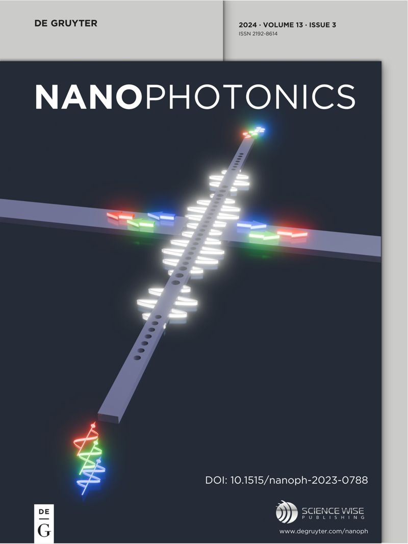
Nanophotonics
Nanophotonics NANOSCIENCE & NANOTECHNOLOGY-MATERIALS SCIENCE, MULTIDISCIPLINARY
CiteScore
13.50
自引率
6.70%
发文量
358
审稿时长
7 weeks
期刊介绍: Nanophotonics, published in collaboration with Sciencewise, is a prestigious journal that showcases recent international research results, notable advancements in the field, and innovative applications. It is regarded as one of the leading publications in the realm of nanophotonics and encompasses a range of article types including research articles, selectively invited reviews, letters, and perspectives. The journal specifically delves into the study of photon interaction with nano-structures, such as carbon nano-tubes, nano metal particles, nano crystals, semiconductor nano dots, photonic crystals, tissue, and DNA. It offers comprehensive coverage of the most up-to-date discoveries, making it an essential resource for physicists, engineers, and material scientists.
×
引用
GB/T 7714-2015
复制
MLA
复制
APA
复制
导出至
BibTeX EndNote RefMan NoteFirst NoteExpress
×
提示
您的信息不完整,为了账户安全,请先补充。
现在去补充
×
提示
您因"违规操作"
具体请查看互助需知
我知道了
×
提示
确定
请完成安全验证×
copy
已复制链接
快去分享给好友吧!
我知道了
右上角分享
点击右上角分享
0
联系我们:info@booksci.cn Book学术提供免费学术资源搜索服务,方便国内外学者检索中英文文献。致力于提供最便捷和优质的服务体验。 Copyright © 2023 布克学术 All rights reserved.
京ICP备2023020795号-1
ghs 京公网安备 11010802042870号
Book学术文献互助
Book学术文献互助群
群 号:481959085
Book学术官方微信