All-2D CVD-grown semiconductor field-effect transistors with van der Waals graphene contacts

IF 9.1 2区 材料科学 Q1 MATERIALS SCIENCE, MULTIDISCIPLINARY
Md. Anamul Hoque, Antony George, Vasudev Ramachandra, Emad Najafidehaghani, Ziyang Gan, Richa Mitra, Bing Zhao, Satyaprakash Sahoo, Maria Abrahamsson, Qiuhua Liang, Julia Wiktor, Andrey Turchanin, Sergey Kubatkin, Samuel Lara-Avila, Saroj P. Dash
{"title":"All-2D CVD-grown semiconductor field-effect transistors with van der Waals graphene contacts","authors":"Md. Anamul Hoque, Antony George, Vasudev Ramachandra, Emad Najafidehaghani, Ziyang Gan, Richa Mitra, Bing Zhao, Satyaprakash Sahoo, Maria Abrahamsson, Qiuhua Liang, Julia Wiktor, Andrey Turchanin, Sergey Kubatkin, Samuel Lara-Avila, Saroj P. Dash","doi":"10.1038/s41699-024-00489-2","DOIUrl":null,"url":null,"abstract":"Two-dimensional (2D) semiconductors and van der Waals (vdW) heterostructures with graphene have generated enormous interest for future electronic, optoelectronic, and energy-harvesting applications. The electronic transport properties and correlations of such hybrid devices strongly depend on the quality of the materials via chemical vapor deposition (CVD) process, their interfaces and contact properties. However, detailed electronic transport and correlation properties of the 2D semiconductor field-effect transistor (FET) with vdW graphene contacts for understanding mobility limiting factors and metal-insulator transition properties are not explored. Here, we investigate electronic transport in scalable all-2D CVD-grown molybdenum disulfide (MoS2) FET with graphene contacts. The Fermi level of graphene can be readily tuned by a gate voltage to enable a nearly perfect band alignment and, hence, a reduced and tunable Schottky barrier at the contact with good field-effect channel mobility. Detailed temperature-dependent transport measurements show dominant phonon/impurity scattering as a mobility limiting mechanisms and a gate-and bias-induced metal-insulator transition in different temperature ranges, which is explained in light of the variable-range hopping transport. These studies in such scalable all-2D semiconductor heterostructure FETs will be useful for future electronic and optoelectronic devices for a broad range of applications.","PeriodicalId":19227,"journal":{"name":"npj 2D Materials and Applications","volume":" ","pages":"1-7"},"PeriodicalIF":9.1000,"publicationDate":"2024-08-21","publicationTypes":"Journal Article","fieldsOfStudy":null,"isOpenAccess":false,"openAccessPdf":"https://www.nature.com/articles/s41699-024-00489-2.pdf","citationCount":"0","resultStr":null,"platform":"Semanticscholar","paperid":null,"PeriodicalName":"npj 2D Materials and Applications","FirstCategoryId":"88","ListUrlMain":"https://www.nature.com/articles/s41699-024-00489-2","RegionNum":2,"RegionCategory":"材料科学","ArticlePicture":[],"TitleCN":null,"AbstractTextCN":null,"PMCID":null,"EPubDate":"","PubModel":"","JCR":"Q1","JCRName":"MATERIALS SCIENCE, MULTIDISCIPLINARY","Score":null,"Total":0}
引用次数: 0

Abstract

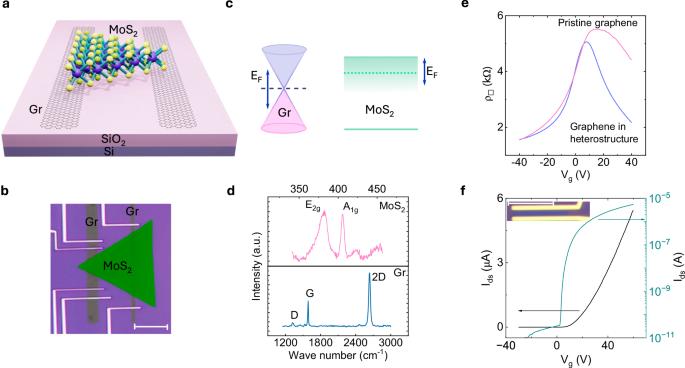
Two-dimensional (2D) semiconductors and van der Waals (vdW) heterostructures with graphene have generated enormous interest for future electronic, optoelectronic, and energy-harvesting applications. The electronic transport properties and correlations of such hybrid devices strongly depend on the quality of the materials via chemical vapor deposition (CVD) process, their interfaces and contact properties. However, detailed electronic transport and correlation properties of the 2D semiconductor field-effect transistor (FET) with vdW graphene contacts for understanding mobility limiting factors and metal-insulator transition properties are not explored. Here, we investigate electronic transport in scalable all-2D CVD-grown molybdenum disulfide (MoS2) FET with graphene contacts. The Fermi level of graphene can be readily tuned by a gate voltage to enable a nearly perfect band alignment and, hence, a reduced and tunable Schottky barrier at the contact with good field-effect channel mobility. Detailed temperature-dependent transport measurements show dominant phonon/impurity scattering as a mobility limiting mechanisms and a gate-and bias-induced metal-insulator transition in different temperature ranges, which is explained in light of the variable-range hopping transport. These studies in such scalable all-2D semiconductor heterostructure FETs will be useful for future electronic and optoelectronic devices for a broad range of applications.
Abstract Image

带有范德华石墨烯触点的全二维 CVD 生长半导体场效应晶体管
二维(2D)半导体和范德华(vdW)异质结构与石墨烯在未来的电子、光电和能量收集应用中产生了巨大的兴趣。这类混合器件的电子传输特性和相关性在很大程度上取决于通过化学气相沉积(CVD)工艺获得的材料的质量、它们的界面和接触特性。然而,目前还没有研究具有 vdW 石墨烯接触的二维半导体场效应晶体管 (FET) 的详细电子传输和相关特性,以了解迁移率限制因素和金属-绝缘体转换特性。在此,我们研究了具有石墨烯触点的可扩展全二维 CVD 生长二硫化钼(MoS2)场效应晶体管的电子传输。石墨烯的费米级可通过栅极电压轻松调节,从而实现近乎完美的带对齐,进而在接触处形成减小且可调的肖特基势垒,并具有良好的场效应沟道迁移率。与温度相关的详细传输测量结果表明,声子/杂质散射是限制迁移率的主要机制,而且在不同温度范围内会出现栅极和偏压诱导的金属-绝缘体转变,这可以根据变程跳变传输来解释。对这种可扩展的全二维半导体异质结构场效应晶体管的研究将有助于未来电子和光电器件的广泛应用。
本文章由计算机程序翻译,如有差异,请以英文原文为准。
求助全文
约1分钟内获得全文 求助全文
来源期刊
npj 2D Materials and Applications
npj 2D Materials and Applications Engineering-Mechanics of Materials
CiteScore
14.50
自引率
2.10%
发文量
80
审稿时长
15 weeks
期刊介绍: npj 2D Materials and Applications publishes papers on the fundamental behavior, synthesis, properties and applications of existing and emerging 2D materials. By selecting papers with the potential for impact, the journal aims to facilitate the transfer of the research of 2D materials into wide-ranging applications.
×
引用
GB/T 7714-2015
复制
MLA
复制
APA
复制
导出至
BibTeX EndNote RefMan NoteFirst NoteExpress
×
提示
您的信息不完整,为了账户安全,请先补充。
现在去补充
×
提示
您因"违规操作"
具体请查看互助需知
我知道了
×
提示
确定
请完成安全验证×
copy
已复制链接
快去分享给好友吧!
我知道了
右上角分享
点击右上角分享
0
联系我们:info@booksci.cn Book学术提供免费学术资源搜索服务,方便国内外学者检索中英文文献。致力于提供最便捷和优质的服务体验。 Copyright © 2023 布克学术 All rights reserved.
京ICP备2023020795号-1
ghs 京公网安备 11010802042870号
Book学术文献互助
Book学术文献互助群
群 号:481959085
Book学术官方微信