Interaction of an Electromagnetic H-Wave with an “Insulator–Semiconductor–Insulator” Nanostructure in the View of Semiconductor Band Structure Anisotropy
{"title":"Interaction of an Electromagnetic H-Wave with an “Insulator–Semiconductor–Insulator” Nanostructure in the View of Semiconductor Band Structure Anisotropy","authors":"I. A. Kuznetsova, O. V. Savenko","doi":"10.1134/S0030400X24020127","DOIUrl":null,"url":null,"abstract":"<p>The problem of electromagnetic H-wave interaction with a layered “insulator–semiconductor–insulator” nanostructure is solved. We assume that the semiconductor layer thickness can be comparable to or less than the charge carrier de Broglie wavelength. Charge carrier surface scattering is taken into account by the Soffer boundary conditions. The electromagnetic wave frequency is less than the plasma resonance frequency. The constant energy surface is an ellipsoid of revolution. Analytical expressions are obtained for the reflection, transmission and absorption coefficients. Calculations are performed for the limiting cases of a degenerate and nondegenerate electron gas. We analyze the dependences of the optical coefficients on dimensionless parameters: the semiconductor layer thickness, the electromagnetic wave frequency and incidence angle, the chemical potential, the ellipticity parameter, the insulating layer permittivities, and the “semiconductor–insulator” interface roughness parameters.</p>","PeriodicalId":723,"journal":{"name":"Optics and Spectroscopy","volume":"132 2","pages":"162 - 169"},"PeriodicalIF":0.9000,"publicationDate":"2024-08-07","publicationTypes":"Journal Article","fieldsOfStudy":null,"isOpenAccess":false,"openAccessPdf":"","citationCount":"0","resultStr":null,"platform":"Semanticscholar","paperid":null,"PeriodicalName":"Optics and Spectroscopy","FirstCategoryId":"101","ListUrlMain":"https://link.springer.com/article/10.1134/S0030400X24020127","RegionNum":4,"RegionCategory":"物理与天体物理","ArticlePicture":[],"TitleCN":null,"AbstractTextCN":null,"PMCID":null,"EPubDate":"","PubModel":"","JCR":"Q4","JCRName":"OPTICS","Score":null,"Total":0}
引用次数: 0
Abstract
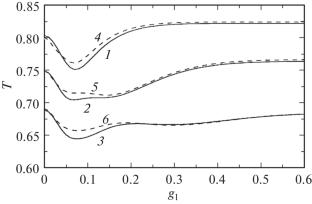
The problem of electromagnetic H-wave interaction with a layered “insulator–semiconductor–insulator” nanostructure is solved. We assume that the semiconductor layer thickness can be comparable to or less than the charge carrier de Broglie wavelength. Charge carrier surface scattering is taken into account by the Soffer boundary conditions. The electromagnetic wave frequency is less than the plasma resonance frequency. The constant energy surface is an ellipsoid of revolution. Analytical expressions are obtained for the reflection, transmission and absorption coefficients. Calculations are performed for the limiting cases of a degenerate and nondegenerate electron gas. We analyze the dependences of the optical coefficients on dimensionless parameters: the semiconductor layer thickness, the electromagnetic wave frequency and incidence angle, the chemical potential, the ellipticity parameter, the insulating layer permittivities, and the “semiconductor–insulator” interface roughness parameters.
期刊介绍:
Optics and Spectroscopy (Optika i spektroskopiya), founded in 1956, presents original and review papers in various fields of modern optics and spectroscopy in the entire wavelength range from radio waves to X-rays. Topics covered include problems of theoretical and experimental spectroscopy of atoms, molecules, and condensed state, lasers and the interaction of laser radiation with matter, physical and geometrical optics, holography, and physical principles of optical instrument making.
 求助内容:
求助内容: 应助结果提醒方式:


