{"title":"High-Performance Low-Voltage Thin-Film Transistors: Experimental and Simulation Validation of Atmospheric Pressure Plasma-Assisted Li<sub>5</sub>AlO<sub>4</sub> Metal Oxide Solution Processing.","authors":"Anand Sharma, Vishwas Acharya, Himanshu Marothya, Satya Veer Singh, Sandeep Kumar, Bhola Nath Pal","doi":"10.1021/acsami.4c05539","DOIUrl":null,"url":null,"abstract":"<p><p>Metal oxide materials processed using solution methods have garnered significant attention due to their ability to efficiently and affordably create transparent insulating layers or active channel layers on various substrates for thin-film transistors (TFTs) used in modern electronics. The key properties of TFTs largely depend on how charge carriers behave near the thin layer at the semiconductor and dielectric interface. Effectively controlling these characteristics offers a straightforward yet effective approach to enhancing device performance. In this study, we propose a novel strategy utilizing atmospheric pressure plasma (APP) treatment to modulate the electrical properties of dielectric thin films and the interfaces between dielectric and semiconductor layers in TFTs processed by using solution methods. Through APP exposure, significant improvements in key TFT parameters were achieved for solution-processed TFTs. Interface states have been reduced from 10<sup>13</sup> to 10<sup>11</sup> cm<sup>-2</sup>, and the on/off current ratio has increased from 10<sup>3</sup> to 10<sup>6</sup> while maintaining a high field-effect mobility of 34 cm<sup>2</sup> V<sup>-1</sup> s<sup>-1</sup>. Additionally, UV-visible spectroscopy and X-ray analysis have confirmed the effectiveness of APP treatment in controlling interface states and traps, leading to overall performance enhancements in the TFTs. Furthermore, our experimental findings have been systematically validated using technology computer-aided design (TCAD) simulations of fabricated TFTs.</p>","PeriodicalId":5,"journal":{"name":"ACS Applied Materials & Interfaces","volume":" ","pages":"43682-43693"},"PeriodicalIF":8.2000,"publicationDate":"2024-08-21","publicationTypes":"Journal Article","fieldsOfStudy":null,"isOpenAccess":false,"openAccessPdf":"","citationCount":"0","resultStr":null,"platform":"Semanticscholar","paperid":null,"PeriodicalName":"ACS Applied Materials & Interfaces","FirstCategoryId":"88","ListUrlMain":"https://doi.org/10.1021/acsami.4c05539","RegionNum":2,"RegionCategory":"材料科学","ArticlePicture":[],"TitleCN":null,"AbstractTextCN":null,"PMCID":null,"EPubDate":"2024/8/9 0:00:00","PubModel":"Epub","JCR":"Q1","JCRName":"MATERIALS SCIENCE, MULTIDISCIPLINARY","Score":null,"Total":0}
引用次数: 0
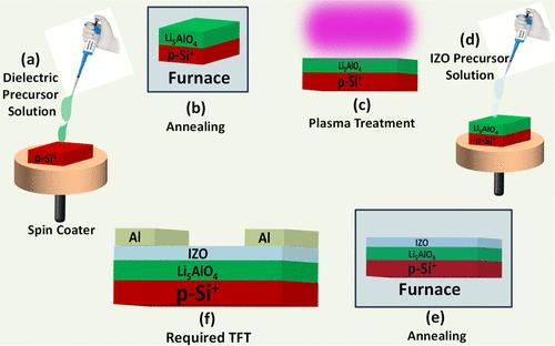
Abstract
Metal oxide materials processed using solution methods have garnered significant attention due to their ability to efficiently and affordably create transparent insulating layers or active channel layers on various substrates for thin-film transistors (TFTs) used in modern electronics. The key properties of TFTs largely depend on how charge carriers behave near the thin layer at the semiconductor and dielectric interface. Effectively controlling these characteristics offers a straightforward yet effective approach to enhancing device performance. In this study, we propose a novel strategy utilizing atmospheric pressure plasma (APP) treatment to modulate the electrical properties of dielectric thin films and the interfaces between dielectric and semiconductor layers in TFTs processed by using solution methods. Through APP exposure, significant improvements in key TFT parameters were achieved for solution-processed TFTs. Interface states have been reduced from 1013 to 1011 cm-2, and the on/off current ratio has increased from 103 to 106 while maintaining a high field-effect mobility of 34 cm2 V-1 s-1. Additionally, UV-visible spectroscopy and X-ray analysis have confirmed the effectiveness of APP treatment in controlling interface states and traps, leading to overall performance enhancements in the TFTs. Furthermore, our experimental findings have been systematically validated using technology computer-aided design (TCAD) simulations of fabricated TFTs.
期刊介绍:
ACS Applied Materials & Interfaces is a leading interdisciplinary journal that brings together chemists, engineers, physicists, and biologists to explore the development and utilization of newly-discovered materials and interfacial processes for specific applications. Our journal has experienced remarkable growth since its establishment in 2009, both in terms of the number of articles published and the impact of the research showcased. We are proud to foster a truly global community, with the majority of published articles originating from outside the United States, reflecting the rapid growth of applied research worldwide.

 求助内容:
求助内容: 应助结果提醒方式:


