Constructing p–n Interfaces to Accelerate Carrier Separation in a Cu2O Photocathode through an In Situ Thermal Oxidation Method for Highly Active Photoelectrochemical Properties
IF 3.4
2区 化学
Q2 CHEMISTRY, MULTIDISCIPLINARY
引用次数: 0
Abstract
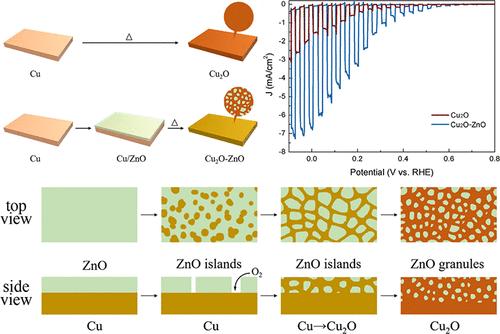
Cu2O-ZnO blended films with the structure of ZnO nanoparticles randomly distributed in the Cu2O matrix were synthesized using an in situ thermal oxidation method. The microstructure and growth mechanism of the prepared Cu2O-ZnO films were revealed depending on elemental mapping and thermogravimetric analysis. Benefiting from the unique structure, an effective built-in electric field formed at the numerous p–n interfaces, enabling efficient spatial separation of carriers. Consequently, photoelectrochemical evaluation of the Cu2O-ZnO film performed under chopped simulated AM 1.5G illumination exhibited a high photocurrent of −6.8 mA/cm2 at 0 V vs RHE, which was 4.5 times higher than that of bare Cu2O film. The onset potential was also positively shifted from 0.62 V vs RHE to 0.74 V vs RHE. The introduction of ZnO also resulted in a high carrier density of 1.96 × 1018 cm–3 and reduced carrier transfer resistance in an electrolyte. To evaluate the potential of long-term application, a 20 nm TiO2 protective layer was deposited by a low energy ion beam technique on the Cu2O-ZnO film; the attenuation of photocurrent was effectively suppressed due to the isolation of the electrolyte. The obtained Cu2O-ZnO blended films with rich p–n interfaces may serve as a good light absorber and carrier provider for use in photoelectric conversion and photoelectrochemical applications.
通过原位热氧化法构建 p-n 接口以加速 Cu2O 阴极中的载流子分离,从而实现高活性光电化学特性
采用原位热氧化法合成了具有 ZnO 纳米颗粒随机分布在 Cu2O 基体中结构的 Cu2O-ZnO 混合薄膜。元素图谱和热重分析揭示了所制备的 Cu2O-ZnO 薄膜的微观结构和生长机制。得益于独特的结构,在众多 p-n 接口上形成了有效的内置电场,从而实现了载流子的有效空间分离。因此,在斩波模拟 AM 1.5G 照明下对 Cu2O-ZnO 薄膜进行的光电化学评估显示,在 0 V 对比 RHE 时,光电流高达 -6.8 mA/cm2,是裸 Cu2O 薄膜的 4.5 倍。起始电位也从 0.62 V vs RHE 正向移动到 0.74 V vs RHE。氧化锌的引入还带来了 1.96 × 1018 cm-3 的高载流子密度,并降低了电解液中的载流子传输电阻。为了评估长期应用的潜力,采用低能量离子束技术在 Cu2O-ZnO 薄膜上沉积了 20 nm 的 TiO2 保护层;由于电解质的隔离,光电流的衰减得到了有效抑制。所获得的具有丰富 p-n 接口的 Cu2O-ZnO 混合薄膜可作为一种良好的光吸收剂和载流子提供者,用于光电转换和光电化学应用。
本文章由计算机程序翻译,如有差异,请以英文原文为准。
求助全文
约1分钟内获得全文
求助全文
来源期刊

Crystal Growth & Design
化学-材料科学:综合
CiteScore
6.30
自引率
10.50%
发文量
650
审稿时长
1.9 months
期刊介绍:
The aim of Crystal Growth & Design is to stimulate crossfertilization of knowledge among scientists and engineers working in the fields of crystal growth, crystal engineering, and the industrial application of crystalline materials.
Crystal Growth & Design publishes theoretical and experimental studies of the physical, chemical, and biological phenomena and processes related to the design, growth, and application of crystalline materials. Synergistic approaches originating from different disciplines and technologies and integrating the fields of crystal growth, crystal engineering, intermolecular interactions, and industrial application are encouraged.
 求助内容:
求助内容: 应助结果提醒方式:


