{"title":"Novel approach to produce 3D boron-doped diamond for pollutant removal from water","authors":"L.G. Vernasqui, A.F. Sardinha, E.J. Corat, N.G. Ferreira","doi":"10.1016/j.cartre.2024.100386","DOIUrl":null,"url":null,"abstract":"<div><p>Diamond growth from Chemical Vapor Deposition (CVD) on foreign substrates can require different pretreatment not only to improve the film nucleation but also to assure its adhesion by decreasing the expected film/substrate interface stress. To improve boron-doped film nucleation, growth, and adherence, different substrate pretreatments have been used mainly from the seeding process with diamond powder at various particle sizes. Despite this, the development of diamond growth on a Ti mesh remains difficult because of the requirement of a cohesive film to cover a 3D macroporous sample with varying growth rates based on its distinct network geometry. Then, this work describes a novel approach to growing boron-doped diamond (BDD) and boron-doped ultrananocrystalline diamond (B-UNCD) on titanium dioxide nanotubes (TDNT) produced simultaneously on both sides of Ti mesh by an anodization process. The films were obtained from two-step growth processes by assuring the entire diamond overlay on both TDNT/Ti mesh sides, including their outer/inner surfaces, as a 3D sample. TiO<sub>2</sub> - TiC conversion has dominated the renucleation process, facilitating the nanometric scale control. The film morphologies were systematically analyzed by FEG-SEM images at different sample planes and depths for both sample sides at different stages of film growth. The unique morphology of titania nanotubes associated with columnar and/or renucleation development of BDD, considering the film defects and valley, can systematically increase the electrode specific area. Raman spectra showed the film quality and its micro and/or ultrananodiamond structure and the boron doping features. Also, this growth process allowed a dopant-controlled adjustable conductivity. Then, the boron doping levels for both films were evaluated from Mott-Schottky plots at around 10<sup>19</sup> Bcm<sup>−3</sup>, characterizing them with good conductivity. In addition, electrochemical measurements from Cyclic Voltammetry (CV) confirmed the expected diamond response on redox pair following the quasi-reversible criteria as high-performance diamond electrodes and in situ Raman spectroelectrochemical measurements assessed the stability of samples during electrochemical measurements, ensuring structural integrity. Finally, the samples were applied to the degradation of methylene blue, proving to be superior materials for electrochemical applications due to their advantages compared to those of similar 2D electrodes.</p></div>","PeriodicalId":52629,"journal":{"name":"Carbon Trends","volume":null,"pages":null},"PeriodicalIF":3.1000,"publicationDate":"2024-07-28","publicationTypes":"Journal Article","fieldsOfStudy":null,"isOpenAccess":false,"openAccessPdf":"https://www.sciencedirect.com/science/article/pii/S2667056924000671/pdfft?md5=22cffc8fbedaac5a3d2b3cdb13939942&pid=1-s2.0-S2667056924000671-main.pdf","citationCount":"0","resultStr":null,"platform":"Semanticscholar","paperid":null,"PeriodicalName":"Carbon Trends","FirstCategoryId":"1085","ListUrlMain":"https://www.sciencedirect.com/science/article/pii/S2667056924000671","RegionNum":0,"RegionCategory":null,"ArticlePicture":[],"TitleCN":null,"AbstractTextCN":null,"PMCID":null,"EPubDate":"","PubModel":"","JCR":"Q2","JCRName":"MATERIALS SCIENCE, MULTIDISCIPLINARY","Score":null,"Total":0}
引用次数: 0
Abstract
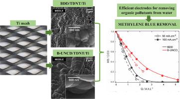
Diamond growth from Chemical Vapor Deposition (CVD) on foreign substrates can require different pretreatment not only to improve the film nucleation but also to assure its adhesion by decreasing the expected film/substrate interface stress. To improve boron-doped film nucleation, growth, and adherence, different substrate pretreatments have been used mainly from the seeding process with diamond powder at various particle sizes. Despite this, the development of diamond growth on a Ti mesh remains difficult because of the requirement of a cohesive film to cover a 3D macroporous sample with varying growth rates based on its distinct network geometry. Then, this work describes a novel approach to growing boron-doped diamond (BDD) and boron-doped ultrananocrystalline diamond (B-UNCD) on titanium dioxide nanotubes (TDNT) produced simultaneously on both sides of Ti mesh by an anodization process. The films were obtained from two-step growth processes by assuring the entire diamond overlay on both TDNT/Ti mesh sides, including their outer/inner surfaces, as a 3D sample. TiO2 - TiC conversion has dominated the renucleation process, facilitating the nanometric scale control. The film morphologies were systematically analyzed by FEG-SEM images at different sample planes and depths for both sample sides at different stages of film growth. The unique morphology of titania nanotubes associated with columnar and/or renucleation development of BDD, considering the film defects and valley, can systematically increase the electrode specific area. Raman spectra showed the film quality and its micro and/or ultrananodiamond structure and the boron doping features. Also, this growth process allowed a dopant-controlled adjustable conductivity. Then, the boron doping levels for both films were evaluated from Mott-Schottky plots at around 1019 Bcm−3, characterizing them with good conductivity. In addition, electrochemical measurements from Cyclic Voltammetry (CV) confirmed the expected diamond response on redox pair following the quasi-reversible criteria as high-performance diamond electrodes and in situ Raman spectroelectrochemical measurements assessed the stability of samples during electrochemical measurements, ensuring structural integrity. Finally, the samples were applied to the degradation of methylene blue, proving to be superior materials for electrochemical applications due to their advantages compared to those of similar 2D electrodes.

 求助内容:
求助内容: 应助结果提醒方式:


