Charge-transfer contacts for the measurement of correlated states in high-mobility WSe2
IF 38.1
1区 材料科学
Q1 MATERIALS SCIENCE, MULTIDISCIPLINARY
引用次数: 0
Abstract
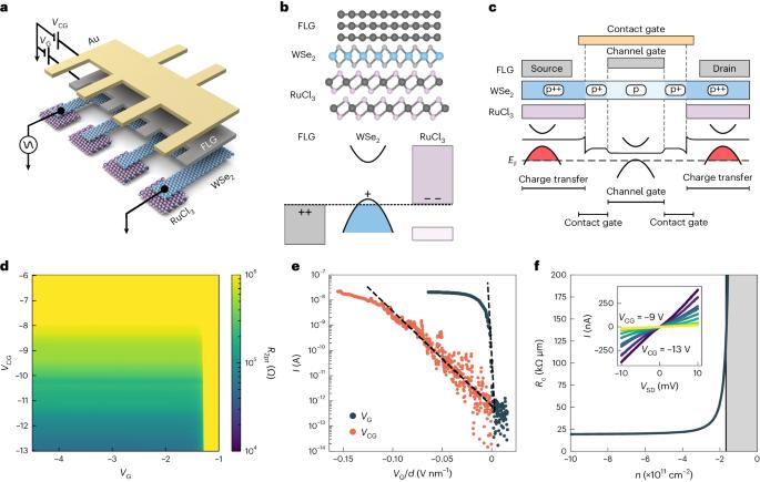
Two-dimensional semiconductors, such as transition metal dichalcogenides, have demonstrated tremendous promise for the development of highly tunable quantum devices. Realizing this potential requires low-resistance electrical contacts that perform well at low temperatures and low densities where quantum properties are relevant. Here we present a new device architecture for two-dimensional semiconductors that utilizes a charge-transfer layer to achieve large hole doping in the contact region, and implement this technique to measure the magnetotransport properties of high-purity monolayer WSe2. We measure a record-high hole mobility of 80,000 cm2 V–1 s–1 and access channel carrier densities as low as 1.6 × 1011 cm−2, an order of magnitude lower than previously achievable. Our ability to realize transparent contact to high-mobility devices at low density enables transport measurements of correlation-driven quantum phases including the observation of a low-temperature metal–insulator transition in a density and temperature regime where Wigner crystal formation is expected and the observation of the fractional quantum Hall effect under large magnetic fields. The charge-transfer contact scheme enables the discovery and manipulation of new quantum phenomena in two-dimensional semiconductors and their heterostructures. By utilizing the van der Waals electron acceptor α-RuCl3, this study establishes a p-type connection with WSe2, facilitating a high hole mobility of 80,000 cm2 V–1 s–1 for investigating quantum transport properties in a magnetic field of over 30 T.


用于测量高迁移率 WSe2 中相关态的电荷转移触点。
二维半导体(如过渡金属二掺镓化合物)在开发高度可调的量子设备方面展现出巨大的潜力。要实现这一潜力,需要在低温和低密度条件下具有良好量子特性的低电阻电接触。在这里,我们介绍了一种利用电荷转移层实现接触区大空穴掺杂的二维半导体新器件结构,并利用这种技术测量了高纯度单层 WSe2 的磁传输特性。我们测得的空穴迁移率达到创纪录的 80,000 cm2 V-1 s-1,通道载流子密度低至 1.6 × 1011 cm-2,比以前可达到的水平低了一个数量级。我们能够在低密度条件下实现与高迁移率器件的透明接触,从而能够进行相关驱动量子相的传输测量,包括在预计会形成维格纳晶体的密度和温度条件下观察到低温金属-绝缘体转变,以及在大磁场条件下观察到分数量子霍尔效应。电荷转移接触方案有助于发现和操纵二维半导体及其异质结构中的新量子现象。
本文章由计算机程序翻译,如有差异,请以英文原文为准。
求助全文
约1分钟内获得全文
求助全文
来源期刊

Nature nanotechnology
工程技术-材料科学:综合
CiteScore
59.70
自引率
0.80%
发文量
196
审稿时长
4-8 weeks
期刊介绍:
Nature Nanotechnology is a prestigious journal that publishes high-quality papers in various areas of nanoscience and nanotechnology. The journal focuses on the design, characterization, and production of structures, devices, and systems that manipulate and control materials at atomic, molecular, and macromolecular scales. It encompasses both bottom-up and top-down approaches, as well as their combinations.
Furthermore, Nature Nanotechnology fosters the exchange of ideas among researchers from diverse disciplines such as chemistry, physics, material science, biomedical research, engineering, and more. It promotes collaboration at the forefront of this multidisciplinary field. The journal covers a wide range of topics, from fundamental research in physics, chemistry, and biology, including computational work and simulations, to the development of innovative devices and technologies for various industrial sectors such as information technology, medicine, manufacturing, high-performance materials, energy, and environmental technologies. It includes coverage of organic, inorganic, and hybrid materials.
 求助内容:
求助内容: 应助结果提醒方式:


