Second harmonic generation in monolithic gallium phosphide metasurfaces

IF 6.5 2区 物理与天体物理 Q1 MATERIALS SCIENCE, MULTIDISCIPLINARY
Muyi Yang, Maximilian A. Weissflog, Zlata Fedorova, Angela I. Barreda, Stefan Börner, Falk Eilenberger, Thomas Pertsch, Isabelle Staude
{"title":"Second harmonic generation in monolithic gallium phosphide metasurfaces","authors":"Muyi Yang, Maximilian A. Weissflog, Zlata Fedorova, Angela I. Barreda, Stefan Börner, Falk Eilenberger, Thomas Pertsch, Isabelle Staude","doi":"10.1515/nanoph-2024-0177","DOIUrl":null,"url":null,"abstract":"Gallium phosphide (GaP) offers unique opportunities for nonlinear and quantum nanophotonics due to its wide optical transparency range, high second-order nonlinear susceptibility, and the possibility to tailor the nonlinear response by a suitable choice of crystal orientation. However, the availability of single crystalline thin films of GaP on low index substrates, as typically required for nonlinear dielectric metasurfaces, is limited. Here we designed and experimentally realized monolithic GaP metasurfaces for enhanced and tailored second harmonic generation (SHG). We fabricated the metasurfaces from bulk (110) GaP wafers using electron-beam lithography and an optimized inductively coupled plasma etching process without a hard mask. SHG measurements showed a high NIR-to-visible conversion efficiency reaching up to 10<jats:sup>−5</jats:sup>, at the same level as typical values for thin-film-based metasurface designs based on III–V semiconductors. Furthermore, using nonlinear back-focal plane imaging, we showed that a significant fraction of the second harmonic was emitted into the zeroth diffraction order along the optical axis. Our results demonstrate that monolithic GaP metasurfaces are a simple and broadly accessible alternative to corresponding thin film designs for many applications in nonlinear nanophotonics.","PeriodicalId":19027,"journal":{"name":"Nanophotonics","volume":"37 1","pages":""},"PeriodicalIF":6.5000,"publicationDate":"2024-07-11","publicationTypes":"Journal Article","fieldsOfStudy":null,"isOpenAccess":false,"openAccessPdf":"","citationCount":"0","resultStr":null,"platform":"Semanticscholar","paperid":null,"PeriodicalName":"Nanophotonics","FirstCategoryId":"101","ListUrlMain":"https://doi.org/10.1515/nanoph-2024-0177","RegionNum":2,"RegionCategory":"物理与天体物理","ArticlePicture":[],"TitleCN":null,"AbstractTextCN":null,"PMCID":null,"EPubDate":"","PubModel":"","JCR":"Q1","JCRName":"MATERIALS SCIENCE, MULTIDISCIPLINARY","Score":null,"Total":0}
引用次数: 0

Abstract

Gallium phosphide (GaP) offers unique opportunities for nonlinear and quantum nanophotonics due to its wide optical transparency range, high second-order nonlinear susceptibility, and the possibility to tailor the nonlinear response by a suitable choice of crystal orientation. However, the availability of single crystalline thin films of GaP on low index substrates, as typically required for nonlinear dielectric metasurfaces, is limited. Here we designed and experimentally realized monolithic GaP metasurfaces for enhanced and tailored second harmonic generation (SHG). We fabricated the metasurfaces from bulk (110) GaP wafers using electron-beam lithography and an optimized inductively coupled plasma etching process without a hard mask. SHG measurements showed a high NIR-to-visible conversion efficiency reaching up to 10−5, at the same level as typical values for thin-film-based metasurface designs based on III–V semiconductors. Furthermore, using nonlinear back-focal plane imaging, we showed that a significant fraction of the second harmonic was emitted into the zeroth diffraction order along the optical axis. Our results demonstrate that monolithic GaP metasurfaces are a simple and broadly accessible alternative to corresponding thin film designs for many applications in nonlinear nanophotonics.
单片磷化镓超表面中的二次谐波生成
磷化镓(GaP)具有宽广的光学透明度范围、高二阶非线性电感以及通过适当选择晶体取向来定制非线性响应的可能性,因此为非线性和量子纳米光子学提供了独特的机遇。然而,非线性介电元表面通常需要的低折射率基底上的 GaP 单晶薄膜的可用性却很有限。在此,我们设计并通过实验实现了用于增强和定制二次谐波发生(SHG)的单片 GaP 元表面。我们利用电子束光刻技术和优化的电感耦合等离子体蚀刻工艺,在没有硬掩膜的情况下,从块状 (110) GaP 硅片上制作了元表面。SHG测量结果表明,近红外到可见光的转换效率高达10-5,与基于III-V族半导体的薄膜基元表面设计的典型值处于同一水平。此外,利用非线性背焦面成像技术,我们发现有相当一部分二次谐波沿光轴向第零衍射阶发射。我们的研究结果表明,在非线性纳米光子学的许多应用中,单片 GaP 元表面是相应薄膜设计的一种简单而广泛的替代方案。
本文章由计算机程序翻译,如有差异,请以英文原文为准。
求助全文
约1分钟内获得全文 求助全文
来源期刊
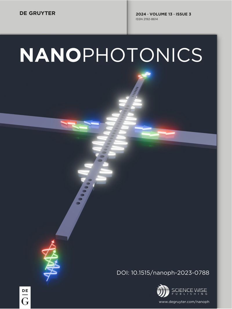
Nanophotonics
Nanophotonics NANOSCIENCE & NANOTECHNOLOGY-MATERIALS SCIENCE, MULTIDISCIPLINARY
CiteScore
13.50
自引率
6.70%
发文量
358
审稿时长
7 weeks
期刊介绍: Nanophotonics, published in collaboration with Sciencewise, is a prestigious journal that showcases recent international research results, notable advancements in the field, and innovative applications. It is regarded as one of the leading publications in the realm of nanophotonics and encompasses a range of article types including research articles, selectively invited reviews, letters, and perspectives. The journal specifically delves into the study of photon interaction with nano-structures, such as carbon nano-tubes, nano metal particles, nano crystals, semiconductor nano dots, photonic crystals, tissue, and DNA. It offers comprehensive coverage of the most up-to-date discoveries, making it an essential resource for physicists, engineers, and material scientists.
×
引用
GB/T 7714-2015
复制
MLA
复制
APA
复制
导出至
BibTeX EndNote RefMan NoteFirst NoteExpress
×
提示
您的信息不完整,为了账户安全,请先补充。
现在去补充
×
提示
您因"违规操作"
具体请查看互助需知
我知道了
×
提示
确定
请完成安全验证×
copy
已复制链接
快去分享给好友吧!
我知道了
右上角分享
点击右上角分享
0
联系我们:info@booksci.cn Book学术提供免费学术资源搜索服务,方便国内外学者检索中英文文献。致力于提供最便捷和优质的服务体验。 Copyright © 2023 布克学术 All rights reserved.
京ICP备2023020795号-1
ghs 京公网安备 11010802042870号
Book学术文献互助
Book学术文献互助群
群 号:481959085
Book学术官方微信