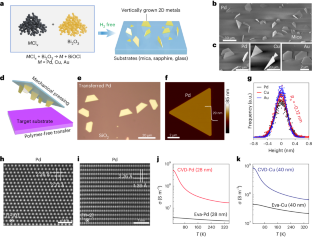
Vertically grown metal nanosheets integrated with atomic-layer-deposited dielectrics for transistors with subnanometre capacitance-equivalent thicknesses
IF 33.7
1区 工程技术
Q1 ENGINEERING, ELECTRICAL & ELECTRONIC
引用次数: 0
Abstract
Integrating thin atomic-layer-deposited dielectrics with two-dimensional (2D) semiconductors could be used to fabricate 2D transistors with sub-1 nm capacitance-equivalent thicknesses. However, non-uniform nucleation from atomic-layer deposition on inert surfaces and subsequent high-energy metal evaporation can make atomically thin dielectrics non-insulating. Here, we report a bismuth-oxide-assisted chemical vapour deposition method to synthesize single-crystalline metal nanosheets with atomically flat surfaces. The nanosheets grow vertically on a substrate and can be easily transferred to a target substrate through polymer-free mechanical pressing. We show that palladium nanosheets offer an excellent surface for atomic-layer deposition of flat aluminium oxide (Al2O3) and hafnium oxide (HfO2) dielectrics with sub-3 nm thicknesses. These can then be laminated onto few-layer molybdenum disulfide (MoS2) as a gate stack with a capacitance-equivalent thickness of 0.9 nm and a capacitance density of around 3.9 μF cm−2. Our MoS2 top-gated transistors with a 2-nm-thick Al2O3 or HfO2 dielectric exhibit leakage currents of 10−6 A cm−2, low operating voltages of around 0.45 V and a hysteresis of less than 1 mV. Vertical metal nanosheets with atomically flat surfaces grown with a bismuth-oxide-assisted chemical vapour deposition method can be used to make metal–oxide dielectric stacks and laminated onto two-dimensional semiconductors to create transistors with sub-1 nm capacitance-equivalent thicknesses.


垂直生长的金属纳米片与原子层沉积电介质的集成,用于具有亚纳米电容等效厚度的晶体管
将原子层沉积的薄电介质与二维(2D)半导体整合在一起,可用于制造电容等效厚度小于 1 纳米的二维晶体管。然而,原子层沉积在惰性表面上的不均匀成核以及随后的高能金属蒸发会使原子薄介电材料失去绝缘性。在此,我们报告了一种氧化铋辅助化学气相沉积方法,用于合成具有原子平整表面的单晶金属纳米片。纳米片垂直生长在基底上,并可通过无聚合物机械压制轻松转移到目标基底上。我们的研究表明,钯纳米片是原子层沉积厚度小于 3 纳米的平面氧化铝(Al2O3)和氧化铪(HfO2)电介质的绝佳表面。然后,这些电介质可以层叠在少层二硫化钼(MoS2)上,作为栅极堆栈,其电容等效厚度为 0.9 纳米,电容密度约为 3.9 μF cm-2。我们的 MoS2 顶部栅极晶体管采用 2 纳米厚的 Al2O3 或 HfO2 电介质,漏电流为 10-6 A cm-2,工作电压低至 0.45 V 左右,滞后小于 1 mV。
本文章由计算机程序翻译,如有差异,请以英文原文为准。
求助全文
约1分钟内获得全文
求助全文
来源期刊

Nature Electronics
Engineering-Electrical and Electronic Engineering
CiteScore
47.50
自引率
2.30%
发文量
159
期刊介绍:
Nature Electronics is a comprehensive journal that publishes both fundamental and applied research in the field of electronics. It encompasses a wide range of topics, including the study of new phenomena and devices, the design and construction of electronic circuits, and the practical applications of electronics. In addition, the journal explores the commercial and industrial aspects of electronics research.
The primary focus of Nature Electronics is on the development of technology and its potential impact on society. The journal incorporates the contributions of scientists, engineers, and industry professionals, offering a platform for their research findings. Moreover, Nature Electronics provides insightful commentary, thorough reviews, and analysis of the key issues that shape the field, as well as the technologies that are reshaping society.
Like all journals within the prestigious Nature brand, Nature Electronics upholds the highest standards of quality. It maintains a dedicated team of professional editors and follows a fair and rigorous peer-review process. The journal also ensures impeccable copy-editing and production, enabling swift publication. Additionally, Nature Electronics prides itself on its editorial independence, ensuring unbiased and impartial reporting.
In summary, Nature Electronics is a leading journal that publishes cutting-edge research in electronics. With its multidisciplinary approach and commitment to excellence, the journal serves as a valuable resource for scientists, engineers, and industry professionals seeking to stay at the forefront of advancements in the field.
 求助内容:
求助内容: 应助结果提醒方式:


