Amit Kumar Verma, Rachana Gupta, Shashi Prakash, Andrei Gloskovskii, Shailesh Kalal, Priyanshi Tiwari, Varimalla Raghavendra Reddy, Rajeev Rawat, Mukul Gupta
{"title":"Structure and Superconductivity of Epitaxial and Polycrystalline VN Thin Films","authors":"Amit Kumar Verma, Rachana Gupta, Shashi Prakash, Andrei Gloskovskii, Shailesh Kalal, Priyanshi Tiwari, Varimalla Raghavendra Reddy, Rajeev Rawat, Mukul Gupta","doi":"10.1021/acsaelm.4c00540","DOIUrl":null,"url":null,"abstract":"In this work, we present a systematic study of superconducting vanadium mononitride (VN) thin films that were simultaneously grown on single crystalline MgO (100) and amorphous SiO<sub>2</sub> substrates. The structure of both samples was probed using X-ray diffraction measurements under different geometries, i.e., specular, off-specular, and ϕ-scan. It was found that the lattice parameter (LP) of VN films grown on SiO<sub>2</sub> was 4.098(7) Å, while on MgO, it was slightly larger at 4.124(2) Å. Though the LP of both samples is within the experimentally obtained and theoretically predicted values, the obtained difference suggests that the polycrystalline VN has a tensile strain as compared to the epitaxial film. The effect of such strain is more clearly reflected on the superconducting transition temperature (<i>T</i><sub>C</sub>) and normal state electrical resistivity (ρ<sub><i>n</i></sub>). In case of the epitaxial VN sample, the <i>T</i><sub>C</sub> was at 8.1 K, while in the polycrystalline sample, it was at 5.2 K. The ρ<sub><i>n</i></sub> was also found to be significantly smaller in epitaxial films, suggesting a better crystalline quality. We performed X-ray absorption and hard X-ray photoelectron spectroscopy measurements to probe the electronic structure. It was found that the surface region of polycrystalline or epitaxial samples remains unaffected by such strains. However, high magnetic field resistivity measurements exhibited a two-step <i>T</i><sub>C</sub> in the epitaxial film which originates due to formation of a thin strained region formed during the initial stages of growth. Our in situ reflection high energy electron diffraction measurements confirmed that the initial stages of growth is strained due to lattice mismatch of about +2.13% between MgO and VN. Overall, this comparative study of epitaxial and polycrystalline samples elucidates the role of stress and strain on the structural, electronic, and superconducting properties of VN thin films.","PeriodicalId":3,"journal":{"name":"ACS Applied Electronic Materials","volume":null,"pages":null},"PeriodicalIF":4.3000,"publicationDate":"2024-06-25","publicationTypes":"Journal Article","fieldsOfStudy":null,"isOpenAccess":false,"openAccessPdf":"","citationCount":"0","resultStr":null,"platform":"Semanticscholar","paperid":null,"PeriodicalName":"ACS Applied Electronic Materials","FirstCategoryId":"88","ListUrlMain":"https://doi.org/10.1021/acsaelm.4c00540","RegionNum":3,"RegionCategory":"材料科学","ArticlePicture":[],"TitleCN":null,"AbstractTextCN":null,"PMCID":null,"EPubDate":"","PubModel":"","JCR":"Q1","JCRName":"ENGINEERING, ELECTRICAL & ELECTRONIC","Score":null,"Total":0}
引用次数: 0
Abstract
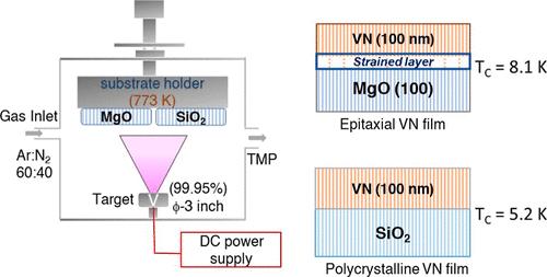
In this work, we present a systematic study of superconducting vanadium mononitride (VN) thin films that were simultaneously grown on single crystalline MgO (100) and amorphous SiO2 substrates. The structure of both samples was probed using X-ray diffraction measurements under different geometries, i.e., specular, off-specular, and ϕ-scan. It was found that the lattice parameter (LP) of VN films grown on SiO2 was 4.098(7) Å, while on MgO, it was slightly larger at 4.124(2) Å. Though the LP of both samples is within the experimentally obtained and theoretically predicted values, the obtained difference suggests that the polycrystalline VN has a tensile strain as compared to the epitaxial film. The effect of such strain is more clearly reflected on the superconducting transition temperature (TC) and normal state electrical resistivity (ρn). In case of the epitaxial VN sample, the TC was at 8.1 K, while in the polycrystalline sample, it was at 5.2 K. The ρn was also found to be significantly smaller in epitaxial films, suggesting a better crystalline quality. We performed X-ray absorption and hard X-ray photoelectron spectroscopy measurements to probe the electronic structure. It was found that the surface region of polycrystalline or epitaxial samples remains unaffected by such strains. However, high magnetic field resistivity measurements exhibited a two-step TC in the epitaxial film which originates due to formation of a thin strained region formed during the initial stages of growth. Our in situ reflection high energy electron diffraction measurements confirmed that the initial stages of growth is strained due to lattice mismatch of about +2.13% between MgO and VN. Overall, this comparative study of epitaxial and polycrystalline samples elucidates the role of stress and strain on the structural, electronic, and superconducting properties of VN thin films.
 求助内容:
求助内容: 应助结果提醒方式:


