Surface Morphology Evolution of MoS2–x by Growth Temperature and Its Effect on Photodetector Properties
IF 4.3
3区 材料科学
Q1 ENGINEERING, ELECTRICAL & ELECTRONIC
引用次数: 0
Abstract
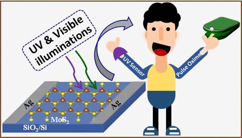
MoS2, being an attractive two-dimensional (2-D) material, has gradually become a research hotspot in recent years. Herein, the MoS2–x thin films are grown through a chemical vapor deposition technique by varying the sulfurization temperature from 700 to 900 °C. X-ray diffraction profile reveals the highly crystalline nature of the sample grown at 800 °C and results in the improved directional orientation of the atoms. A decrement in the intensity of the S 2p peak for the thin film sulfurized at 800 °C signifies the diffusion of the sulfur atoms into the molybdenum atoms, prominently resulting in the development of a nanostructured morphology. The formation of an ohmic contact between the photoactive material and the electrode results in the fast transportation of the charge carriers through the metal-semiconductor interface. The sample grown at 800 °C, achieves a high photocurrent, a sharp rise time, and a superior responsivity of 112.49 μA, 35 ms, and 2.69 A/W, respectively, under the illumination of the visible light (λ = 550 nm) and optical power density of 0.1667 mW/cm2 attributed to its higher crystalline nature and formation of prominent nanoflake-structured morphology. Finally, with superior figures of merit, the fabricated photodetector signifies its potential for application in optoelectronics devices.
生长温度对 MoS2-x 表面形态的影响及其对光电探测器性能的影响
MoS2 是一种极具吸引力的二维(2-D)材料,近年来逐渐成为研究热点。本文采用化学气相沉积技术,通过改变硫化温度(700 至 900 °C)来生长 MoS2-x 薄膜。X 射线衍射图显示了 800 °C 下生长的样品的高结晶性,并改善了原子的定向取向。在 800 ℃ 下硫化的薄膜的 S 2p 峰强度降低,表明硫原子扩散到了钼原子中,显著形成了纳米结构形态。光活性材料与电极之间形成的欧姆接触使电荷载流子能够快速通过金属-半导体界面。在可见光(λ = 550 nm)和 0.1667 mW/cm2 光功率密度的照射下,在 800 °C 下生长的样品实现了较高的光电流、较快的上升时间和较高的响应率,分别为 112.49 μA、35 ms 和 2.69 A/W ,这归功于其较高的结晶性和突出的纳米片结构形态的形成。最后,所制造的光电探测器具有优异的性能数据,表明其在光电设备中的应用潜力。
本文章由计算机程序翻译,如有差异,请以英文原文为准。
求助全文
约1分钟内获得全文
求助全文

 求助内容:
求助内容: 应助结果提醒方式:


