Integrated 1D epitaxial mirror twin boundaries for ultrascaled 2D MoS2 field-effect transistors
IF 38.1
1区 材料科学
Q1 MATERIALS SCIENCE, MULTIDISCIPLINARY
引用次数: 0
Abstract
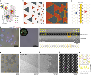
In atomically thin van der Waals materials, grain boundaries—the line defects between adjacent crystal grains with tilted in-plane rotations—are omnipresent. When the tilting angles are arbitrary, the grain boundaries form inhomogeneous sublattices, giving rise to local electronic states that are not controlled. Here we report on epitaxial realizations of deterministic MoS2 mirror twin boundaries (MTBs) at which two adjoining crystals are reflection mirroring by an exactly 60° rotation by position-controlled epitaxy. We showed that these epitaxial MTBs are one-dimensionally metallic to a circuit length scale. By utilizing the ultimate one-dimensional (1D) feature (width ~0.4 nm and length up to a few tens of micrometres), we incorporated the epitaxial MTBs as a 1D gate to build integrated two-dimensional field-effect transistors (FETs). The critical role of the 1D MTB gate was verified to scale the depletion channel length down to 3.9 nm, resulting in a substantially lowered channel off-current at lower gate voltages. With that, in both individual and array FETs, we demonstrated state-of-the-art performances for low-power logics. The 1D epitaxial MTB gates in this work suggest a novel synthetic pathway for the integration of two-dimensional FETs—that are immune to high gate capacitance—towards ultimate scaling. Mirror twin boundaries in monolayer MoS2—line defects with reflection-mirroring symmetry—are one-dimensionally metallic. In this work, the authors fabricate these mirror twin boundary networks by epitaxity and incorporate them into ultrascaled 2D transistor circuits as gate electrodes.
超大规模二维 MoS2 场效应晶体管的集成一维外延镜像孪生边界
在原子薄范德华材料中,晶界--相邻晶粒之间具有倾斜平面旋转的线缺陷--无处不在。当倾斜角为任意角度时,晶界会形成不均匀的亚晶格,从而产生不受控制的局部电子态。在这里,我们报告了确定性 MoS2 镜像孪晶边界(MTB)的外延实现情况,在这种情况下,两个相邻晶体通过位置控制外延,以精确 60° 旋转的方式实现反射镜像。我们的研究表明,这些外延 MTB 在电路长度尺度上具有一维金属性。通过利用最终的一维(1D)特征(宽度约为 0.4 纳米,长度可达几十微米),我们将外延 MTB 作为一维栅极来构建集成的二维场效应晶体管(FET)。通过验证,一维 MTB 栅极的关键作用是将耗尽沟道长度缩减到 3.9 纳米,从而在较低栅极电压下大幅降低沟道关断电流。因此,在单个和阵列场效应晶体管中,我们展示了低功耗逻辑器件的一流性能。这项工作中的一维外延 MTB 栅极为二维场效应晶体管的集成提供了一种新的合成途径,这种场效应晶体管不受高栅极电容的影响,可实现最终的扩展。
本文章由计算机程序翻译,如有差异,请以英文原文为准。
求助全文
约1分钟内获得全文
求助全文
来源期刊
Nature nanotechnology
工程技术-材料科学:综合
CiteScore
59.70
自引率
0.80%
发文量
196
审稿时长
4-8 weeks
期刊介绍:
Nature Nanotechnology is a prestigious journal that publishes high-quality papers in various areas of nanoscience and nanotechnology. The journal focuses on the design, characterization, and production of structures, devices, and systems that manipulate and control materials at atomic, molecular, and macromolecular scales. It encompasses both bottom-up and top-down approaches, as well as their combinations.
Furthermore, Nature Nanotechnology fosters the exchange of ideas among researchers from diverse disciplines such as chemistry, physics, material science, biomedical research, engineering, and more. It promotes collaboration at the forefront of this multidisciplinary field. The journal covers a wide range of topics, from fundamental research in physics, chemistry, and biology, including computational work and simulations, to the development of innovative devices and technologies for various industrial sectors such as information technology, medicine, manufacturing, high-performance materials, energy, and environmental technologies. It includes coverage of organic, inorganic, and hybrid materials.
文献相关原料
| 公司名称 | 产品信息 | 采购帮参考价格 |
|---|
 求助内容:
求助内容: 应助结果提醒方式:


