{"title":"Light-Triggered Anti-ambipolar Transistor Based on an In-Plane Lateral Homojunction","authors":"Hecheng Han, Baoqing Zhang, Zihao Zhang, Yiming Wang, Chuan Liu, Arun Kumar Singh, Aimin Song, Yuxiang Li*, Jidong Jin* and Jiawei Zhang*, ","doi":"10.1021/acs.nanolett.4c01679","DOIUrl":null,"url":null,"abstract":"<p >Currently, the construction of anti-ambipolar transistors (AATs) is primarily based on asymmetric heterostructures, which are challenging to fabricate. AATs used for photodetection are accompanied by dark currents that prove difficult to suppress, resulting in reduced sensitivity. This work presents light-triggered AATs based on an in-plane lateral WSe<sub>2</sub> homojunction without van der Waals heterostructures. In this device, the WSe<sub>2</sub> channel is partially electrically controlled by the back gate due to the screening effect of the bottom electrode, resulting in a homojunction that is dynamically modulated with gate voltage, exhibiting electrostatically reconfigurable and light-triggered anti-ambipolar behaviors. It exhibits high responsivity (188 A/W) and detectivity (8.94 × 10<sup>14</sup> Jones) under 635 nm illumination with a low power density of 0.23 μW/cm<sup>2</sup>, promising a new approach to low-power, high-performance photodetectors. Moreover, the device demonstrates efficient self-driven photodetection. Furthermore, ternary inverters are realized using monolithic WSe<sub>2</sub>, simplifying the manufacturing of multivalued logic devices.</p>","PeriodicalId":53,"journal":{"name":"Nano Letters","volume":null,"pages":null},"PeriodicalIF":9.6000,"publicationDate":"2024-07-02","publicationTypes":"Journal Article","fieldsOfStudy":null,"isOpenAccess":false,"openAccessPdf":"","citationCount":"0","resultStr":null,"platform":"Semanticscholar","paperid":null,"PeriodicalName":"Nano Letters","FirstCategoryId":"88","ListUrlMain":"https://pubs.acs.org/doi/10.1021/acs.nanolett.4c01679","RegionNum":1,"RegionCategory":"材料科学","ArticlePicture":[],"TitleCN":null,"AbstractTextCN":null,"PMCID":null,"EPubDate":"","PubModel":"","JCR":"Q1","JCRName":"CHEMISTRY, MULTIDISCIPLINARY","Score":null,"Total":0}
引用次数: 0
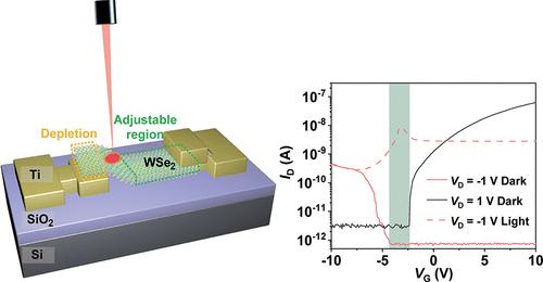
Abstract
Currently, the construction of anti-ambipolar transistors (AATs) is primarily based on asymmetric heterostructures, which are challenging to fabricate. AATs used for photodetection are accompanied by dark currents that prove difficult to suppress, resulting in reduced sensitivity. This work presents light-triggered AATs based on an in-plane lateral WSe2 homojunction without van der Waals heterostructures. In this device, the WSe2 channel is partially electrically controlled by the back gate due to the screening effect of the bottom electrode, resulting in a homojunction that is dynamically modulated with gate voltage, exhibiting electrostatically reconfigurable and light-triggered anti-ambipolar behaviors. It exhibits high responsivity (188 A/W) and detectivity (8.94 × 10¹⁴ Jones) under 635 nm illumination with a low power density of 0.23 μW/cm2, promising a new approach to low-power, high-performance photodetectors. Moreover, the device demonstrates efficient self-driven photodetection. Furthermore, ternary inverters are realized using monolithic WSe2, simplifying the manufacturing of multivalued logic devices.
期刊介绍:
Nano Letters serves as a dynamic platform for promptly disseminating original results in fundamental, applied, and emerging research across all facets of nanoscience and nanotechnology. A pivotal criterion for inclusion within Nano Letters is the convergence of at least two different areas or disciplines, ensuring a rich interdisciplinary scope. The journal is dedicated to fostering exploration in diverse areas, including:
- Experimental and theoretical findings on physical, chemical, and biological phenomena at the nanoscale
- Synthesis, characterization, and processing of organic, inorganic, polymer, and hybrid nanomaterials through physical, chemical, and biological methodologies
- Modeling and simulation of synthetic, assembly, and interaction processes
- Realization of integrated nanostructures and nano-engineered devices exhibiting advanced performance
- Applications of nanoscale materials in living and environmental systems
Nano Letters is committed to advancing and showcasing groundbreaking research that intersects various domains, fostering innovation and collaboration in the ever-evolving field of nanoscience and nanotechnology.


 求助内容:
求助内容: 应助结果提醒方式:


