Large-area solution-processable black phosphorus for electronic application
IF 2.6
Q3 MATERIALS SCIENCE, MULTIDISCIPLINARY
引用次数: 0
Abstract
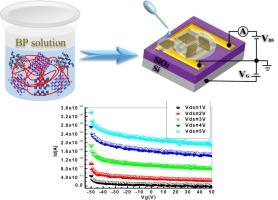
Two-dimensional (2D) layered black phosphorus (BP), with a direct band gap and high carrier mobility, has shown great potential for next generation electronics and optoelectronics. However, how to prepare a large-area 2D material film is still a big problem for realizing its practical applications. Herein, an improved one-step solution-processable method is put forward to solving this problem to get uniform and large-area BP film. Our results show that the designed electrodes can be fully covered by BP flakes and the corresponding FET reveals relatively high performance. Our study opens a new avenue in fabricating large-area ultra-thin BP films.
用于电子应用的大面积可溶液加工黑磷
二维(2D)层状黑磷(BP)具有直接带隙和高载流子迁移率,在下一代电子学和光电子学领域显示出巨大的潜力。然而,如何制备大面积的二维材料薄膜仍是实现其实际应用的一大难题。为解决这一问题,本文提出了一种改进的一步溶液可加工方法,以获得均匀的大面积 BP 薄膜。我们的研究结果表明,所设计的电极可以被 BP 片完全覆盖,相应的场效应晶体管也显示出了相对较高的性能。我们的研究为制造大面积超薄 BP 薄膜开辟了一条新途径。
本文章由计算机程序翻译,如有差异,请以英文原文为准。
求助全文
约1分钟内获得全文
求助全文

 求助内容:
求助内容: 应助结果提醒方式:


