Exciton–Phonon Coupling Induces a New Pathway for Ultrafast Intralayer-to-Interlayer Exciton Transition and Interlayer Charge Transfer in WS2–MoS2 Heterostructure: A First-Principles Study
Yang-hao Chan*, Mit H. Naik, Jonah B. Haber, Jeffrey B. Neaton, Steven G. Louie, Diana Y. Qiu* and Felipe H. da Jornada*,
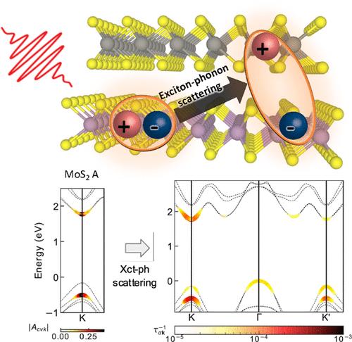
{"title":"Exciton–Phonon Coupling Induces a New Pathway for Ultrafast Intralayer-to-Interlayer Exciton Transition and Interlayer Charge Transfer in WS2–MoS2 Heterostructure: A First-Principles Study","authors":"Yang-hao Chan*, Mit H. Naik, Jonah B. Haber, Jeffrey B. Neaton, Steven G. Louie, Diana Y. Qiu* and Felipe H. da Jornada*, ","doi":"10.1021/acs.nanolett.4c01508","DOIUrl":null,"url":null,"abstract":"<p >Despite the weak, van der Waals interlayer coupling, photoinduced charge transfer vertically across atomically thin interfaces can occur within surprisingly fast, sub-50 fs time scales. An early theoretical understanding of charge transfer is based on a noninteracting picture, neglecting excitonic effects that dominate optical properties of such materials. We employ an <i>ab initio</i> many-body perturbation theory approach, which explicitly accounts for the excitons and phonons in the heterostructure. Our large-scale first-principles calculations directly probe the role of exciton–phonon coupling in the charge dynamics of the WS<sub>2</sub>/MoS<sub>2</sub> heterobilayer. We find that the exciton–phonon interaction induced relaxation time of photoexcited excitons at the <i>K</i> valley of MoS<sub>2</sub> and WS<sub>2</sub> is 67 and 15 fs at 300 K, respectively, which sets a lower bound to the intralayer-to-interlayer exciton transfer time and is consistent with experiment reports. We further show that electron–hole correlations facilitate novel transfer pathways that are otherwise inaccessible to noninteracting electrons and holes.</p>","PeriodicalId":53,"journal":{"name":"Nano Letters","volume":null,"pages":null},"PeriodicalIF":9.6000,"publicationDate":"2024-06-18","publicationTypes":"Journal Article","fieldsOfStudy":null,"isOpenAccess":false,"openAccessPdf":"https://pubs.acs.org/doi/epdf/10.1021/acs.nanolett.4c01508","citationCount":"0","resultStr":null,"platform":"Semanticscholar","paperid":null,"PeriodicalName":"Nano Letters","FirstCategoryId":"88","ListUrlMain":"https://pubs.acs.org/doi/10.1021/acs.nanolett.4c01508","RegionNum":1,"RegionCategory":"材料科学","ArticlePicture":[],"TitleCN":null,"AbstractTextCN":null,"PMCID":null,"EPubDate":"","PubModel":"","JCR":"Q1","JCRName":"CHEMISTRY, MULTIDISCIPLINARY","Score":null,"Total":0}
引用次数: 0
Abstract
Despite the weak, van der Waals interlayer coupling, photoinduced charge transfer vertically across atomically thin interfaces can occur within surprisingly fast, sub-50 fs time scales. An early theoretical understanding of charge transfer is based on a noninteracting picture, neglecting excitonic effects that dominate optical properties of such materials. We employ an ab initio many-body perturbation theory approach, which explicitly accounts for the excitons and phonons in the heterostructure. Our large-scale first-principles calculations directly probe the role of exciton–phonon coupling in the charge dynamics of the WS2/MoS2 heterobilayer. We find that the exciton–phonon interaction induced relaxation time of photoexcited excitons at the K valley of MoS2 and WS2 is 67 and 15 fs at 300 K, respectively, which sets a lower bound to the intralayer-to-interlayer exciton transfer time and is consistent with experiment reports. We further show that electron–hole correlations facilitate novel transfer pathways that are otherwise inaccessible to noninteracting electrons and holes.
期刊介绍:
Nano Letters serves as a dynamic platform for promptly disseminating original results in fundamental, applied, and emerging research across all facets of nanoscience and nanotechnology. A pivotal criterion for inclusion within Nano Letters is the convergence of at least two different areas or disciplines, ensuring a rich interdisciplinary scope. The journal is dedicated to fostering exploration in diverse areas, including:
- Experimental and theoretical findings on physical, chemical, and biological phenomena at the nanoscale
- Synthesis, characterization, and processing of organic, inorganic, polymer, and hybrid nanomaterials through physical, chemical, and biological methodologies
- Modeling and simulation of synthetic, assembly, and interaction processes
- Realization of integrated nanostructures and nano-engineered devices exhibiting advanced performance
- Applications of nanoscale materials in living and environmental systems
Nano Letters is committed to advancing and showcasing groundbreaking research that intersects various domains, fostering innovation and collaboration in the ever-evolving field of nanoscience and nanotechnology.


 求助内容:
求助内容: 应助结果提醒方式:


