Field emission from two-dimensional (2D) CdSSe flake flowers structure grown on gold coated silicon substrate: An efficient cold cathode
Abstract
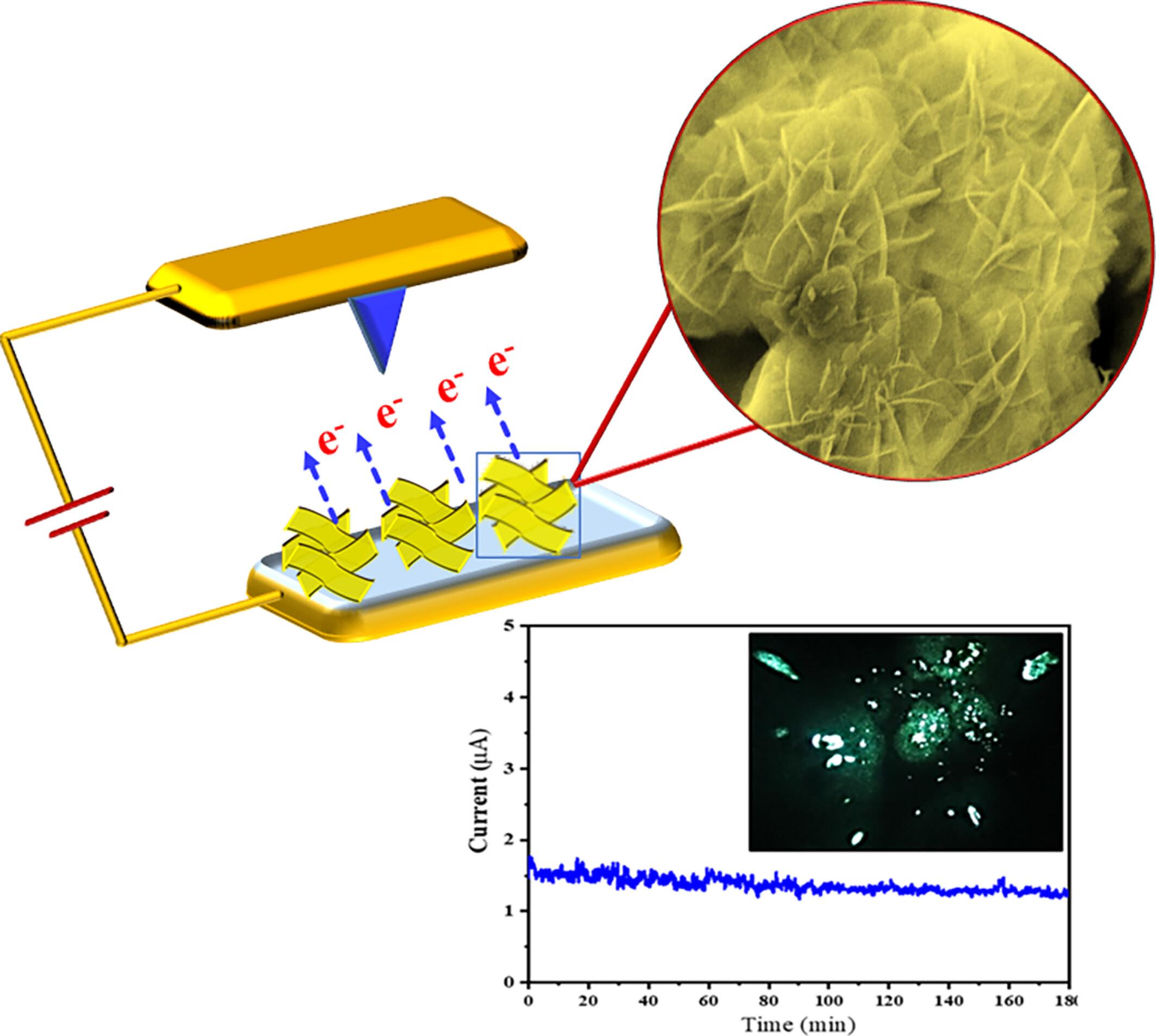
Field emission finds a vital space in numerous scientific and technological applications, including high-resolution imaging at micro- and nano-scales, conducting high-energy physics experiments, molecule ionization in spectroscopy, and electronic uses. A continuous effort exists to develop new materials for enhanced field emission applications. In the present work, two-dimensional (2D) well-aligned CdSSe flake flowers (CdSSe-FFs) were successfully grown on gold-coated silicon substrate utilizing a simple and affordable chemical bath deposition approach at ambient temperature. The time-dependent growth mechanism from nanoparticles to FFs was observed at optimized parameters such as concentration of precursors, pH (~11), deposition time, and solution temperature. The crystalline nature of CdSSe-FFs is confirmed by high-resolution transmission electron microscopy (HRTEM) results, and selected area electron diffraction (SAED) observations reveal a hexagonal crystal structure. Additionally, the CdSSe-FFs thickness was confirmed by TEM analysis and found to be ~20–30 nm. The optical, photoelectric, and field emission (FE) characteristics are thoroughly explored which shows significant enhancement due to the formation of heterojunction between the gold-coated silicon substrate and CdSSe-FFs. The UV–visible absorption spectra of CdSSe-FFs show enhanced absorption at 700 nm, corresponding to the energy band gap (Eg) of 1.77 eV. The CdSSe-FFs exhibited field emission and photosensitive field emission (PSFE) characteristics. In FE study CdSSe-FFs shows an increase in current density of 387.2 μ A cm−2 in an applied field of 4.1 V m−1 which is 4.08 fold as compared to without light illumination (95.1 μ A cm−2). Furthermore, it shows excellent emission current stability at the preset value of 1.5 μA over 3 h with a deviation of the current density of less than 5% respectively.
Research Highlights
- Novel CdSSe flake flowers were grown on Au-coated Si substrate by a cost-effective chemical bath deposition route.
- The growth mechanism of CdSSe flake flowers is studied in detail.
- Field emission and Photoluminescence study of CdSSe flake flowers is characterized.
- CdSSe flake flowers with nanoflakes sharp edges exhibited enhanced field emission properties.
 求助内容:
求助内容: 应助结果提醒方式:


