G. Hari Priya , S.K. Srivastava , M.V. Shankar , K.M.K. Srivatsa , Amish G. Joshi , Koteswara Rao Peta
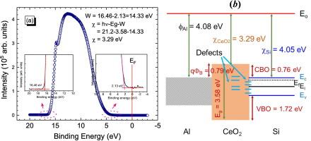
{"title":"Tuning of interface quality of Al/CeO2/Si device by post-annealing of sol-gel grown high-k CeO2 layers","authors":"G. Hari Priya , S.K. Srivastava , M.V. Shankar , K.M.K. Srivatsa , Amish G. Joshi , Koteswara Rao Peta","doi":"10.1016/j.mee.2024.112212","DOIUrl":null,"url":null,"abstract":"<div><p>A comprehensive study has been done on the influence of post-deposition annealing temperature on high-k cerium oxide (CeO<sub>2</sub>) layer grown on n-type silicon (Si) substrate and its resultant interface states have been studied for Al/CeO<sub>2</sub>/Si metal-oxide-semiconductor (MOS) devices. The high-k CeO<sub>2</sub> thin films were deposited by spin-coating and sintered at different annealing temperatures (<em>T</em><sub><em>a</em></sub>) in the range of 400–900 °C. The parameters such as fixed charge density (<em>Q</em><sub><em>eff</em></sub>), dielectric constant (<em>k</em>) of the layers, flat-band voltage (<em>V</em><sub><em>FB</em></sub>), interface defect density (D<sub><em>it</em></sub>), etc., of the MOS device were evaluated from C<img>V and I-V measurements. A minimum value of flat band shift (∼0.05 V) with lower <em>Q</em><sub><em>eff</em></sub> (−4.81 × 10<sup>11</sup> C/cm<sup>2</sup>) have been achieved for the <em>T</em><sub><em>a</em></sub> of 600 °C. The <em>k</em> and <em>D</em><sub><em>it</em></sub> were evaluated to be 22 and 1.29 × 10<sup>12</sup> cm<sup>−2</sup>, respectively at the <em>T</em><sub><em>a</em></sub> of 600 °C. In addition, the C<img>V measurements showed a very small hysteresis and very low frequency dispersion for the <em>T</em><sub><em>a</em></sub> of 600 °C sample. Energy distribution of defect states was evaluated and it was maximum towards the bottom of the conduction band. This shows that the 600 °C is the optimum annealing temperature, which results in high quality interface, and the electron affinity of the corresponding CeO<sub>2</sub> layers was found to be 3.29 eV as evaluated from ultraviolet photoelectron spectroscopy (UPS). Further, a maximum value of minority carrier lifetime (147 μs) has been achieved for the samples annealed at <em>T</em><sub><em>a</em></sub> of 400 °C, indicating that the post-annealing temperature plays a significant role on the properties of CeO<sub>2</sub> films deposited by sol-gel process. Thus, the present study demonstrates the possibility of sol-gel grown high k-CeO<sub>2</sub> layers suitable for MOS like devices.</p></div>","PeriodicalId":18557,"journal":{"name":"Microelectronic Engineering","volume":"292 ","pages":"Article 112212"},"PeriodicalIF":3.1000,"publicationDate":"2024-05-28","publicationTypes":"Journal Article","fieldsOfStudy":null,"isOpenAccess":false,"openAccessPdf":"","citationCount":"0","resultStr":null,"platform":"Semanticscholar","paperid":null,"PeriodicalName":"Microelectronic Engineering","FirstCategoryId":"5","ListUrlMain":"https://www.sciencedirect.com/science/article/pii/S0167931724000819","RegionNum":4,"RegionCategory":"工程技术","ArticlePicture":[],"TitleCN":null,"AbstractTextCN":null,"PMCID":null,"EPubDate":"","PubModel":"","JCR":"Q2","JCRName":"ENGINEERING, ELECTRICAL & ELECTRONIC","Score":null,"Total":0}
引用次数: 0
Abstract
A comprehensive study has been done on the influence of post-deposition annealing temperature on high-k cerium oxide (CeO2) layer grown on n-type silicon (Si) substrate and its resultant interface states have been studied for Al/CeO2/Si metal-oxide-semiconductor (MOS) devices. The high-k CeO2 thin films were deposited by spin-coating and sintered at different annealing temperatures (Ta) in the range of 400–900 °C. The parameters such as fixed charge density (Qeff), dielectric constant (k) of the layers, flat-band voltage (VFB), interface defect density (Dit), etc., of the MOS device were evaluated from CV and I-V measurements. A minimum value of flat band shift (∼0.05 V) with lower Qeff (−4.81 × 10¹¹ C/cm2) have been achieved for the Ta of 600 °C. The k and Dit were evaluated to be 22 and 1.29 × 1012 cm−2, respectively at the Ta of 600 °C. In addition, the CV measurements showed a very small hysteresis and very low frequency dispersion for the Ta of 600 °C sample. Energy distribution of defect states was evaluated and it was maximum towards the bottom of the conduction band. This shows that the 600 °C is the optimum annealing temperature, which results in high quality interface, and the electron affinity of the corresponding CeO2 layers was found to be 3.29 eV as evaluated from ultraviolet photoelectron spectroscopy (UPS). Further, a maximum value of minority carrier lifetime (147 μs) has been achieved for the samples annealed at Ta of 400 °C, indicating that the post-annealing temperature plays a significant role on the properties of CeO2 films deposited by sol-gel process. Thus, the present study demonstrates the possibility of sol-gel grown high k-CeO2 layers suitable for MOS like devices.
期刊介绍:
Microelectronic Engineering is the premier nanoprocessing, and nanotechnology journal focusing on fabrication of electronic, photonic, bioelectronic, electromechanic and fluidic devices and systems, and their applications in the broad areas of electronics, photonics, energy, life sciences, and environment. It covers also the expanding interdisciplinary field of "more than Moore" and "beyond Moore" integrated nanoelectronics / photonics and micro-/nano-/bio-systems. Through its unique mixture of peer-reviewed articles, reviews, accelerated publications, short and Technical notes, and the latest research news on key developments, Microelectronic Engineering provides comprehensive coverage of this exciting, interdisciplinary and dynamic new field for researchers in academia and professionals in industry.

 求助内容:
求助内容: 应助结果提醒方式:


