Nicholas Hunwick, Xiaolei Liu, Mustafa Togay, John M. Walls, Jake Bowers and Patrick J. M. Isherwood
{"title":"The effect of oxygen on NiO as a back buffer layer in CdTe solar cells","authors":"Nicholas Hunwick, Xiaolei Liu, Mustafa Togay, John M. Walls, Jake Bowers and Patrick J. M. Isherwood","doi":"10.1039/D4YA00125G","DOIUrl":null,"url":null,"abstract":"<p >Thin film CdTe-based photovoltaic devices have achieved high efficiency above 22%. However, the device performance is limited by large open circuit voltage deficit. One of the primary reasons is non-ohmic back contacts. In this work, nickel oxide is used as a back buffer layer to form an ohmic back contact. We comprehensively investigate oxygen effects during sputtering on film properties and device performance. Increased oxygen in the deposition environment led to darker films, increased carrier concentration, decreased mobility and decreased resistivity. X-ray photoelectron spectroscopy showed peak shifts favouring Ni<small><sup>3+</sup></small> over Ni<small><sup>2+</sup></small>, and X-ray diffraction demonstrated that crystallinity hit a peak at around 5% oxygen input. The NiO back buffer layer improves device performance by reducing barrier height at the gold back contact and improving valence band offset at the CdTe/NiO interface. The NiO layer deposited without oxygen improved the <em>V</em><small><sub>oc</sub></small> to 710 mV, from a baseline of 585 mV. At 5% and 20% oxygen content during deposition, efficiency improved relative to the reference due to an increase in open circuit voltage (<em>V</em><small><sub>oc</sub></small>) and short circuit current (<em>J</em><small><sub>sc</sub></small>). <em>V</em><small><sub>oc</sub></small> increase is due to improved valence band offset between CdTe and NiO. The large conduction band offset also reflects minority carriers away from the CdTe/NiO interface and reduces interface recombination. SCAPS simulations demonstrated that an increase in valence band offset has shown pronounced effects of both s-kinks and rollover.</p>","PeriodicalId":72913,"journal":{"name":"Energy advances","volume":" 7","pages":" 1746-1753"},"PeriodicalIF":3.2000,"publicationDate":"2024-05-30","publicationTypes":"Journal Article","fieldsOfStudy":null,"isOpenAccess":false,"openAccessPdf":"https://pubs.rsc.org/en/content/articlepdf/2024/ya/d4ya00125g?page=search","citationCount":"0","resultStr":null,"platform":"Semanticscholar","paperid":null,"PeriodicalName":"Energy advances","FirstCategoryId":"1085","ListUrlMain":"https://pubs.rsc.org/en/content/articlelanding/2024/ya/d4ya00125g","RegionNum":0,"RegionCategory":null,"ArticlePicture":[],"TitleCN":null,"AbstractTextCN":null,"PMCID":null,"EPubDate":"","PubModel":"","JCR":"Q2","JCRName":"CHEMISTRY, PHYSICAL","Score":null,"Total":0}
引用次数: 0
Abstract
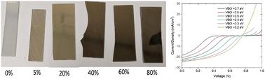
Thin film CdTe-based photovoltaic devices have achieved high efficiency above 22%. However, the device performance is limited by large open circuit voltage deficit. One of the primary reasons is non-ohmic back contacts. In this work, nickel oxide is used as a back buffer layer to form an ohmic back contact. We comprehensively investigate oxygen effects during sputtering on film properties and device performance. Increased oxygen in the deposition environment led to darker films, increased carrier concentration, decreased mobility and decreased resistivity. X-ray photoelectron spectroscopy showed peak shifts favouring Ni3+ over Ni2+, and X-ray diffraction demonstrated that crystallinity hit a peak at around 5% oxygen input. The NiO back buffer layer improves device performance by reducing barrier height at the gold back contact and improving valence band offset at the CdTe/NiO interface. The NiO layer deposited without oxygen improved the Voc to 710 mV, from a baseline of 585 mV. At 5% and 20% oxygen content during deposition, efficiency improved relative to the reference due to an increase in open circuit voltage (Voc) and short circuit current (Jsc). Voc increase is due to improved valence band offset between CdTe and NiO. The large conduction band offset also reflects minority carriers away from the CdTe/NiO interface and reduces interface recombination. SCAPS simulations demonstrated that an increase in valence band offset has shown pronounced effects of both s-kinks and rollover.

 求助内容:
求助内容: 应助结果提醒方式:


