{"title":"Spatially selective p-type doping for constructing lateral WS2 p-n homojunction via low-energy nitrogen ion implantation","authors":"Yufan Kang, Yongfeng Pei, Dong He, Hang Xu, Mingjun Ma, Jialu Yan, Changzhong Jiang, Wenqing Li, Xiangheng Xiao","doi":"10.1038/s41377-024-01477-3","DOIUrl":null,"url":null,"abstract":"<p>The construction of lateral p-n junctions is very important and challenging in two-dimensional (2D) semiconductor manufacturing process. Previous researches have demonstrated that vertical p-n junction can be prepared simply by vertical stacking of 2D materials. However, interface pollution and large area scalability are challenges that are difficult to overcome with vertical stacking technology. Constructing 2D lateral p-n homojunction is an effective strategy to address these issues. Spatially selective p-type doping of 2D semiconductors is expected to construct lateral p-n homojunction. In this work, we have developed a low-energy ion implantation system that reduces the implanted energy to 300 eV. Low-energy implantation can form a shallow implantation depth, which is more suitable for modulating the electrical and optical properties of 2D materials. Hence, we utilize low-energy ion implantation to directly dope nitrogen ions into few-layer WS<sub>2</sub> and successfully realize a precise regulation for WS<sub>2</sub> with its conductivity type transforming from n-type to bipolar or even p-type conduction. Furthermore, the universality of this method is demonstrated by extending it to other 2D semiconductors, including WSe<sub>2</sub>, SnS<sub>2</sub> and MoS<sub>2</sub>. Based on this method, a lateral WS<sub>2</sub> p-n homojunction is fabricated, which exhibits significant rectification characteristics. A photodetector based on p-n junction with photovoltaic effect is also prepared, and the open circuit voltage can reach to 0.39 V. This work provides an effective way for controllable doping of 2D semiconductors.</p>","PeriodicalId":18069,"journal":{"name":"Light-Science & Applications","volume":null,"pages":null},"PeriodicalIF":20.6000,"publicationDate":"2024-05-30","publicationTypes":"Journal Article","fieldsOfStudy":null,"isOpenAccess":false,"openAccessPdf":"","citationCount":"0","resultStr":null,"platform":"Semanticscholar","paperid":null,"PeriodicalName":"Light-Science & Applications","FirstCategoryId":"1089","ListUrlMain":"https://doi.org/10.1038/s41377-024-01477-3","RegionNum":0,"RegionCategory":null,"ArticlePicture":[],"TitleCN":null,"AbstractTextCN":null,"PMCID":null,"EPubDate":"","PubModel":"","JCR":"Q1","JCRName":"OPTICS","Score":null,"Total":0}
引用次数: 0
Abstract
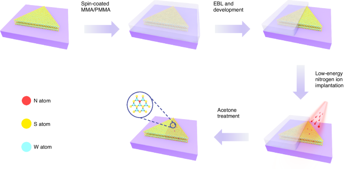
The construction of lateral p-n junctions is very important and challenging in two-dimensional (2D) semiconductor manufacturing process. Previous researches have demonstrated that vertical p-n junction can be prepared simply by vertical stacking of 2D materials. However, interface pollution and large area scalability are challenges that are difficult to overcome with vertical stacking technology. Constructing 2D lateral p-n homojunction is an effective strategy to address these issues. Spatially selective p-type doping of 2D semiconductors is expected to construct lateral p-n homojunction. In this work, we have developed a low-energy ion implantation system that reduces the implanted energy to 300 eV. Low-energy implantation can form a shallow implantation depth, which is more suitable for modulating the electrical and optical properties of 2D materials. Hence, we utilize low-energy ion implantation to directly dope nitrogen ions into few-layer WS2 and successfully realize a precise regulation for WS2 with its conductivity type transforming from n-type to bipolar or even p-type conduction. Furthermore, the universality of this method is demonstrated by extending it to other 2D semiconductors, including WSe2, SnS2 and MoS2. Based on this method, a lateral WS2 p-n homojunction is fabricated, which exhibits significant rectification characteristics. A photodetector based on p-n junction with photovoltaic effect is also prepared, and the open circuit voltage can reach to 0.39 V. This work provides an effective way for controllable doping of 2D semiconductors.
 求助内容:
求助内容: 应助结果提醒方式:


