Yttrium-doping-induced metallization of molybdenum disulfide for ohmic contacts in two-dimensional transistors
IF 40.9
1区 工程技术
Q1 ENGINEERING, ELECTRICAL & ELECTRONIC
引用次数: 0
Abstract
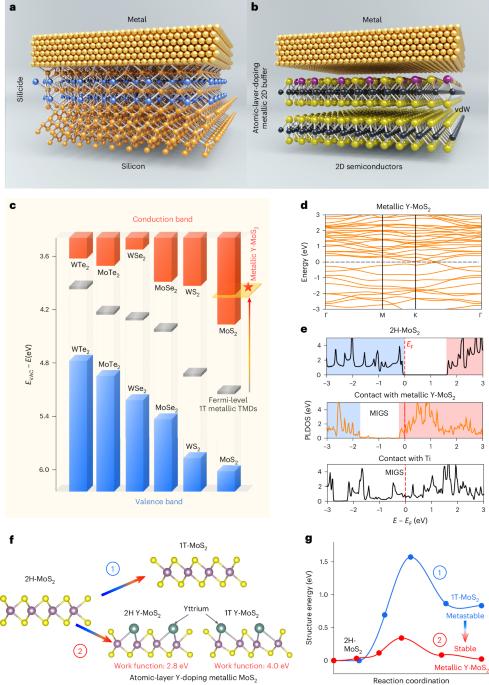
The van der Waals systems could be used to overcome the issue of Fermi-level pinning in contacts of transistors based on two-dimensional semiconductors. However, the lack of advanced-node-lithography-compatible methods limits the use of such materials in wafer-scale integrated manufacturing. Here we report a yttrium-doping approach to convert semiconducting molybdenum disulfide (MoS2) into metallic MoS2. The approach, which is compatible with advanced-node wafer-scale integration, improves the band alignment and provides ohmic device contacts. It is based on a solid-state-source three-step doping method involving plasma, deposition and annealing, and can provide ångström-thickness surface doping. The yttrium-doped MoS2 acts as a metallic buffer that improves charge carrier transfer from the metal electrode to semiconducting MoS2. With this approach, we fabricate self-aligned, 10-nm-channel-length MoS2 field-effect transistors on two-inch wafers with an average contact resistances of 69 Ω µm and total resistances of 235 Ω µm. Our devices exhibit an ON-current density of 1.22 mA µm–1 at a drain voltage of 0.7 V, a ballistic ratio of 79% and a transconductance of 3.2 mS µm–1. A yttrium-doped metallic two-dimensional buffer layer can be used to improve charge carrier transport between the metal contacts and semiconductor channel in molybdenum-disulfide-based transistors.

二硫化钼钇掺杂金属化用于二维晶体管中的欧姆触点
范德华系统可用于克服基于二维半导体的晶体管触点中的费米级针销问题。然而,由于缺乏先进的节点光刻兼容方法,限制了此类材料在晶圆级集成制造中的应用。在此,我们报告了一种将二硫化钼(MoS2)半导体转化为金属 MoS2 的掺钇方法。这种方法与先进的节点晶圆级集成兼容,可改善带排列并提供欧姆器件触点。该方法以固态源三步掺杂法为基础,包括等离子体、沉积和退火,可提供盎司厚度的表面掺杂。掺钇的 MoS2 可充当金属缓冲器,改善电荷载流子从金属电极向半导体 MoS2 的转移。利用这种方法,我们在两英寸晶圆上制造出了自对准、10 纳米沟道长度的 MoS2 场效应晶体管,其平均接触电阻为 69 Ω µm,总电阻为 235 Ω µm。我们的器件在 0.7 V 漏极电压下的导通电流密度为 1.22 mA µm-1,弹道比为 79%,跨导为 3.2 mS µm-1。
本文章由计算机程序翻译,如有差异,请以英文原文为准。
求助全文
约1分钟内获得全文
求助全文
来源期刊
Nature Electronics
Engineering-Electrical and Electronic Engineering
CiteScore
47.50
自引率
2.30%
发文量
159
期刊介绍:
Nature Electronics is a comprehensive journal that publishes both fundamental and applied research in the field of electronics. It encompasses a wide range of topics, including the study of new phenomena and devices, the design and construction of electronic circuits, and the practical applications of electronics. In addition, the journal explores the commercial and industrial aspects of electronics research.
The primary focus of Nature Electronics is on the development of technology and its potential impact on society. The journal incorporates the contributions of scientists, engineers, and industry professionals, offering a platform for their research findings. Moreover, Nature Electronics provides insightful commentary, thorough reviews, and analysis of the key issues that shape the field, as well as the technologies that are reshaping society.
Like all journals within the prestigious Nature brand, Nature Electronics upholds the highest standards of quality. It maintains a dedicated team of professional editors and follows a fair and rigorous peer-review process. The journal also ensures impeccable copy-editing and production, enabling swift publication. Additionally, Nature Electronics prides itself on its editorial independence, ensuring unbiased and impartial reporting.
In summary, Nature Electronics is a leading journal that publishes cutting-edge research in electronics. With its multidisciplinary approach and commitment to excellence, the journal serves as a valuable resource for scientists, engineers, and industry professionals seeking to stay at the forefront of advancements in the field.
 求助内容:
求助内容: 应助结果提醒方式:


