S. Guillemin, L. Lachal, P. Gergaud, A. Grenier, F. Nemouchi, F. Mazen, Ph. Rodriguez
{"title":"A comparative study of C, N and Xe pre-amorphization implantation processes for improving the thermal stability of NiSi films","authors":"S. Guillemin, L. Lachal, P. Gergaud, A. Grenier, F. Nemouchi, F. Mazen, Ph. Rodriguez","doi":"10.1016/j.mee.2024.112210","DOIUrl":null,"url":null,"abstract":"<div><p>In this paper, a comparative study of C-, N- and Xe-based pre-amorphization implantation (PAI) processes is proposed. The impact of the use of such processes on the agglomeration resistance and physical properties of the final Ni(<em>Pt</em>)Si layer, as well as the formation mechanisms via solid-state reactions and electrical performances via the transfer length measurement (TLM) method, is evaluated. It is shown that although all species are able to increase the agglomeration temperature of Ni(<em>Pt</em>)Si layers (up to more than 100 °C), the underlying mechanisms are different. For C- and N-based PAI processes a strong chemical effect is observed, while for Xe-based processes the amorphization depth plays an important role. Consequently, the beneficial effect of stabilizing Ni(<em>Pt</em>)Si layers at high temperatures using C- and N-based PAI processes has to be balanced with an increased layer resistivity (up to 30%) combined with a strong deterioration of the associated specific contact resistivity (which is multiplied by almost a factor 10). In this sense, Xe-based PAI processes seem to be a better option as they could allow to combine both requirements.</p></div>","PeriodicalId":18557,"journal":{"name":"Microelectronic Engineering","volume":"291 ","pages":"Article 112210"},"PeriodicalIF":2.6000,"publicationDate":"2024-05-24","publicationTypes":"Journal Article","fieldsOfStudy":null,"isOpenAccess":false,"openAccessPdf":"","citationCount":"0","resultStr":null,"platform":"Semanticscholar","paperid":null,"PeriodicalName":"Microelectronic Engineering","FirstCategoryId":"5","ListUrlMain":"https://www.sciencedirect.com/science/article/pii/S0167931724000790","RegionNum":4,"RegionCategory":"工程技术","ArticlePicture":[],"TitleCN":null,"AbstractTextCN":null,"PMCID":null,"EPubDate":"","PubModel":"","JCR":"Q2","JCRName":"ENGINEERING, ELECTRICAL & ELECTRONIC","Score":null,"Total":0}
引用次数: 0
Abstract
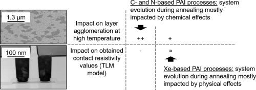
In this paper, a comparative study of C-, N- and Xe-based pre-amorphization implantation (PAI) processes is proposed. The impact of the use of such processes on the agglomeration resistance and physical properties of the final Ni(Pt)Si layer, as well as the formation mechanisms via solid-state reactions and electrical performances via the transfer length measurement (TLM) method, is evaluated. It is shown that although all species are able to increase the agglomeration temperature of Ni(Pt)Si layers (up to more than 100 °C), the underlying mechanisms are different. For C- and N-based PAI processes a strong chemical effect is observed, while for Xe-based processes the amorphization depth plays an important role. Consequently, the beneficial effect of stabilizing Ni(Pt)Si layers at high temperatures using C- and N-based PAI processes has to be balanced with an increased layer resistivity (up to 30%) combined with a strong deterioration of the associated specific contact resistivity (which is multiplied by almost a factor 10). In this sense, Xe-based PAI processes seem to be a better option as they could allow to combine both requirements.
本文对基于 C、N 和 Xe 的预变质植入 (PAI) 工艺进行了比较研究。本文评估了使用这些工艺对最终镍(铂)硅层的抗团聚性和物理性质的影响,以及通过固态反应和转移长度测量(TLM)方法对电性能形成机制的影响。结果表明,尽管所有物种都能提高 Ni(Pt)Si 层的聚结温度(高达 100 ℃ 以上),但其基本机制却各不相同。对于基于 C 和 N 的 PAI 过程,可以观察到强烈的化学效应,而对于基于 Xe 的过程,非晶化深度起着重要作用。因此,使用 C 和 N 基 PAI 工艺在高温下稳定 Ni(Pt)Si 层的有利效果必须与层电阻率的增加(高达 30%)以及相关特定接触电阻率的严重恶化(几乎是 10 倍)相平衡。从这个意义上说,Xe 基 PAI 工艺似乎是一个更好的选择,因为它可以同时满足这两个要求。
期刊介绍:
Microelectronic Engineering is the premier nanoprocessing, and nanotechnology journal focusing on fabrication of electronic, photonic, bioelectronic, electromechanic and fluidic devices and systems, and their applications in the broad areas of electronics, photonics, energy, life sciences, and environment. It covers also the expanding interdisciplinary field of "more than Moore" and "beyond Moore" integrated nanoelectronics / photonics and micro-/nano-/bio-systems. Through its unique mixture of peer-reviewed articles, reviews, accelerated publications, short and Technical notes, and the latest research news on key developments, Microelectronic Engineering provides comprehensive coverage of this exciting, interdisciplinary and dynamic new field for researchers in academia and professionals in industry.

 求助内容:
求助内容: 应助结果提醒方式:


