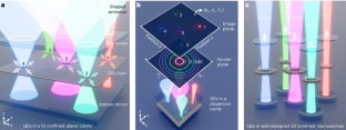
Super-resolved snapshot hyperspectral imaging of solid-state quantum emitters for high-throughput integrated quantum technologies
IF 32.3
1区 物理与天体物理
Q1 OPTICS
引用次数: 0
Abstract
Solid-state quantum emitters coupled to integrated photonic nanostructures are quintessential for exploring fundamental phenomena in cavity quantum electrodynamics and are used in a wide range of photonic quantum technologies. One of the most exciting prospects for integrated photonics is the potential for massive production of miniaturized devices on a single chip. However, the efficiency and reproducibility of light–matter coupling are hindered by the spectral and spatial mismatch between the single solid-state quantum emitters and the optical modes supported by the photonic nanostructures. Here we develop a platform and method for hyperspectral imaging of solid-state quantum emitters to address this long-standing issue. Spatially distributed and spectrally broadened InAs quantum dots are embedded in a GaAs/AlGaAs one-dimensional (1D) planar cavity that consists of two distributed Bragg reflectors acting as mirrors. By exploiting the extended mode of the dispersive 1D cavity and the way it shapes the out-of-plane emission from the quantum dots, we extract the spatial position and emission wavelength of each dot from a single wide-field photoluminescence image, with a spatial and spectral accuracy down to 15 nm and 0.4 nm, respectively. We then fabricate quantum light sources by etching the 1D confined planar cavity into 3D confined micropillars. Extension of this technique using an open planar cavity can be exploited for a variety of compact quantum photonic devices with expanded functionalities for large-scale integration. Our technology is particularly appealing for quantum photonic applications that involve the spatial and spectral characterization of a large number of solid-state quantum emitters. The position and emission wavelengths of single quantum dots embedded in a one-dimensional planar cavity can be simultaneously determined from a single photoluminescence image with 15 nm spatial accuracy and subnanometric spectral accuracy in the near-infrared.


固态量子发射器的超分辨快照高光谱成像,用于高通量集成量子技术
与集成光子纳米结构耦合的固态量子发射器是探索空腔量子电动力学基本现象的关键,并广泛应用于光子量子技术。集成光子学最令人兴奋的前景之一是在单个芯片上大规模生产微型器件的潜力。然而,单个固态量子发射器与光子纳米结构支持的光学模式之间的光谱和空间不匹配阻碍了光物质耦合的效率和可重复性。在此,我们开发了一种固态量子发射器高光谱成像平台和方法,以解决这一长期存在的问题。空间分布和光谱拓宽的砷化镓量子点被嵌入砷化镓/砷化镓一维(1D)平面腔体中,该腔体由两个分布式布拉格反射镜组成。通过利用色散一维空腔的扩展模式及其塑造量子点平面外发射的方式,我们从单个宽场光致发光图像中提取了每个点的空间位置和发射波长,空间和光谱精度分别低至 15 nm 和 0.4 nm。然后,我们将一维约束平面腔蚀刻成三维约束微柱,从而制造出量子光源。利用开放式平面腔体对这一技术进行扩展,可用于各种紧凑型量子光子器件,并为大规模集成提供更多功能。我们的技术对于涉及大量固态量子发射器的空间和光谱表征的量子光子应用尤其具有吸引力。
本文章由计算机程序翻译,如有差异,请以英文原文为准。
求助全文
约1分钟内获得全文
求助全文
来源期刊

Nature Photonics
物理-光学
CiteScore
54.20
自引率
1.70%
发文量
158
审稿时长
12 months
期刊介绍:
Nature Photonics is a monthly journal dedicated to the scientific study and application of light, known as Photonics. It publishes top-quality, peer-reviewed research across all areas of light generation, manipulation, and detection.
The journal encompasses research into the fundamental properties of light and its interactions with matter, as well as the latest developments in optoelectronic devices and emerging photonics applications. Topics covered include lasers, LEDs, imaging, detectors, optoelectronic devices, quantum optics, biophotonics, optical data storage, spectroscopy, fiber optics, solar energy, displays, terahertz technology, nonlinear optics, plasmonics, nanophotonics, and X-rays.
In addition to research papers and review articles summarizing scientific findings in optoelectronics, Nature Photonics also features News and Views pieces and research highlights. It uniquely includes articles on the business aspects of the industry, such as technology commercialization and market analysis, offering a comprehensive perspective on the field.
 求助内容:
求助内容: 应助结果提醒方式:


