Low‐Temperature Epitaxy of Perovskite WO3 Thin Films under Atmospheric Conditions
引用次数: 0
Abstract
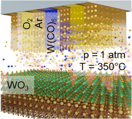
As Si electronics hits fundamental performance limits, oxide integration emerges as a solution to augment the next generation of electronic and optical devices. Specifically, oxide perovskites provide diverse functionalities with a potential to create, tune, and combine emergent phenomena at interfaces. High‐level crystalline order is needed to realize these functionalities, often achieved through epitaxy. However, large‐scale implementation in consumer devices faces challenges due to the need for high‐temperature deposition in complex vacuum systems. Herein, this challenge is addressed using atmospheric pressure spatial chemical vapor deposition, a thin‐film fabrication technique that can rapidly produce uniform films at sub‐400 °C temperatures under atmospheric conditions over ≈cm2 areas. Thus, the deposition of epitaxial perovskite tungsten trioxide, WO3, thin films is demonstrated at a rate of 5 nm min−2 on single‐crystal substrates at 350 °C in open‐air conditions enabling a high‐throughput process. The resulting films exhibit crystallographic and electronic properties comparable to vacuum‐based growth above 500 °C. The high‐quality epitaxy is attributed to the energetics of the exothermic decomposition reaction of the W[CO]6 precursors combined with the stabilization of a hot zone near the substrate surface. From this work, the way can be paved for low‐temperature atmospheric‐pressure epitaxy of a wide range of other perovskite thin films.
大气条件下过氧化物 WO3 薄膜的低温外延
随着硅电子器件的基本性能达到极限,氧化物集成成为增强下一代电子和光学器件的解决方案。具体来说,氧化物包晶提供了多种功能,有可能在界面上创造、调整和组合新出现的现象。要实现这些功能,需要较高的晶序,通常通过外延来实现。然而,由于需要在复杂的真空系统中进行高温沉积,消费类设备的大规模应用面临着挑战。在此,我们采用大气压空间化学气相沉积技术来应对这一挑战,这种薄膜制造技术可在大气条件下以低于 400 °C 的温度在 ≈cm2 的面积上快速生成均匀的薄膜。因此,在 350 °C 的露天条件下,以 5 nm min-2 的速度在单晶基底上沉积外延包晶三氧化钨(WO3)薄膜,实现了高通量工艺。所得薄膜的晶体学和电子特性可与 500 °C 以上的真空生长相媲美。高质量的外延归功于 W[CO]6 前驱体放热分解反应的能量学原理,以及基底表面附近热区的稳定。从这项工作出发,可以为其他各种包晶体薄膜的低温常压外延铺平道路。
本文章由计算机程序翻译,如有差异,请以英文原文为准。
求助全文
约1分钟内获得全文
求助全文

 求助内容:
求助内容: 应助结果提醒方式:


